A similar version of this arTIcle appeared in the November 11, 2007 issue of PET magazine.
Unlike tradiTIonal op amps, the high-side current-sense amplifier doesn't include an internal ESD diode from each input pin to its power-supply pin. As a result, it can operate at common mode voltages well above the level of its VCC supply. Furthermore, pulling the VCC pin of a typical current-sense amplifier to ground places the part in shutdown mode, in which it draws no quiescent current; only leakage current. Thus, the VCC pin of a current-sense amplifier can serve as a shutdown pin.
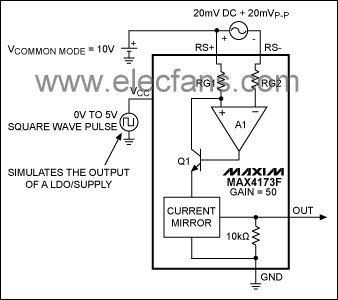
Consider a typical battery-operated device in which a power source (LDO, buck/boost converter, etc.) powers several ICs on a circuit board, including a MAX4173 current-sense amplifier. To extend battery life by saving power, the system frequently turns off the LDOs and current-sense amplifiers. That action is simulated in the circuit of Figure 1.

Figure 1. Zero volts on the VCC pin of a current-sense amplifier (MAX4173 in this case) effectively shuts it down.
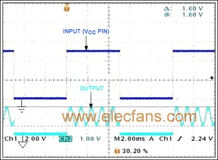
To simulate the signal otherwise obtained by placing a current-sense resistor in the power-supply line, a 20mVP-P signal, offset by 20mV, rides on a 10V common mode input voltage. Loss of VCC is simulated by a 0V-to-5V square wave at the VCC pin. During 5V intervals at VCC the amplifier operates in its active mode, but during 0V intervals it goes into shutdown. Because the amplifier gain is 50, the expected output is 50 × (20mVP-P + 20mV), i.e., a 1VP-P sinewave offset by 1V (Figure 2). As expected, the amplifier is active when 5V is applied and produces the expected output. When VCC goes to 0V the output also goes to 0V. The part shuts down and draws no supply current.

Figure 2. These waveforms illustrate the effect of shutting down a current-sense amplifier using the method shown in Figure 1. The amplifier draws no quiescent current when VCC is 0V.
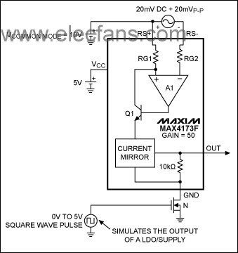
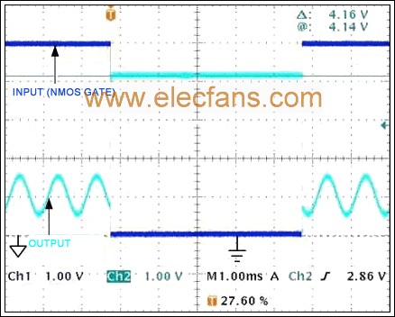
Another way of shutting down a current-sense amplifier is to connect an NMOS transistor in the ground path (Figure 3), and drive it with logic-level signals capable of turning the transistor ON and OFF. When the transistor is ON, the amplifier operates normally. When it's OFF, the amplifier shuts down because its ground is floating. The output waveform for this setup (Figure 4) demonstrates the expected behavior: amplifying the input signal during 5V intervals, and floating close to VCC during 0V intervals. During the shutdown intervals, the leakage current measured at the VCC pin is just 4µA, due to the 1MΩ input impedance of the measurement scope. When the scope probe is absent, only the NMOS transistor's leakage current is drawn from VCC. Input current on the RS+/RS- pins is just 0.3µA.

Figure 3. Opening the GND terminal of a current-sense amplifier also shuts it down.

Figure 4. With the ground connection open, the current-sense amplifier of Figure 3 shuts down, drawing no quiescent current.
Thus, one can easily put the MAX4173 in shutdown mode either by pulling its VCC pin to ground, or by opening its ground connection using an NMOS transistor. Similar results can be expected from other current-sense amplifiers as well.
欢迎分享,转载请注明来源:内存溢出

 微信扫一扫
微信扫一扫
 支付宝扫一扫
评论列表(0条)