
Whether this performance plateau results from a need to keep pace with technology or vice versa, the need for higher supply current in portable systems is forcing designers to become familiar with new power-supply technologies. This article explores some of these new technologies.
Shrinking geometries have consistently driven down the supply voltages for CPUs, DSPs, and other large-scale logic devices. Currently in the +1.5V to +2.5V range, these voltages should soon reach 1V. Efficient generation of voltages this low can be a problem, especially for output currents of 10A and up.
As for most electronic designs, an effective power supply must reconcile numerous conflicting goals including cost and component count, efficiency and thermal behavior, circuit size, and transient performance (response to load steps, etc.). Battery life is an issue for portable (battery-powered) systems only, but waste heat (and therefore efficiency) is a major concern for both battery- and AC-powered systems.
Tighter Load Regulation + Faster Response = A Losing BattleToday's CPU cores require very tight load regulation. Until recently, the major CPU makers demanded exactly that. But the supply current and clock frequency rise as supply voltages fall, and that places acute demands on the power supply—especially with regard to load-step behavior. The growing difficulty and cost of meeting these ever-tighter performance limits has motivated a rethinking of power-supply design. As just one consequence of higher load currents and larger load transients, the capacitor "farms" that sprout up around a processor add size and cost to a design.
These issues, and the fact that even the fastest switch-mode regulators cannot handle the instantaneous output drop caused by a sudden load step, have forced a change of thinking (and specifications). Output capacitors must do all the work in coping with a step response at the speed of today's CPUs. Furthermore, the tighter load-regulation specs that result in higher open-loop gain require more output capacitance to maintain stability. Thus, it became clear that some way of relaxing the demands of load regulation would pay off generously in reduced component count and in other ways as well.
The response of a typical DC-DC converter to a load step (Figure 1) has five basic elements:
- An instantaneous drop, whose magnitude equals the increase in the load-current step multiplied by the output capacitors' equivalent series resistance (ESR).
- After the instantaneous drop, there may be a droop before the DC-DC converter responds, in which capacitor voltage falls as the capacitor supplies load current.
- A voltage-recovery interval, as the inductor switches on to source load current and replenish the output capacitance.
- An "ESR step-up" as the load is removed (reversing the effect of the instantaneous drop).
- Some overshoot, as energy stored in the first inductor pulse (after the load falls) is transferred to the output capacitance.
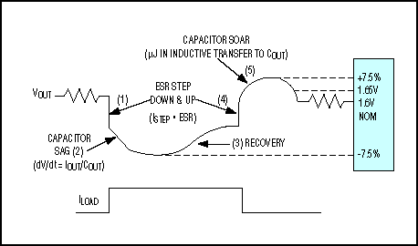
Figure 1. This waveform illustrates the major components of a transient load step.
Voltage Positioning It became clear that flogging a DC-DC converter for unrealistic transient behavior was hopeless. A 600MHz CPU generates 60 clock cycles during the MAX1711's 100ns response time. If the supply voltage always falls by ESRCOUT × ILOAD STEP and stays there for several clock cycles, does it matter whether the output ever returns to its nominal value? From the CPU's standpoint, it doesn't matter. From the power supply's standpoint, however, it matters a lot.
The power supply much prefers that the voltage under load never returns to "nominal." That way, nearly twice as much transient voltage rise can be accommodated when the load is removed. Similarly, twice as much transient drop is allowed when the load is applied. Figure 2 illustrates the different ways a voltage converter can respond to a load step.
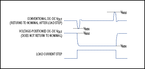
Figure 2. Because voltage-positioned regulators don't attempt to restore the output voltage to a centered "nominal" after each load step, they allow larger transient excursions. This extra margin reduces power consumption and the output-capacitor count as well.
These considerations have led to a new type of specification for CPU power supplies (see the gray box in Figure 1). The nominal voltage is 1.6V, but load-dependent droop can pull it down by 7.5% (quite sloppy by current CPU standards). It can also rise by 7.5% (short-term pulses only) when the load drops from full to zero. Output voltage in the steady state must not exceed 1.65V including noise and ripple. These numbers help minimize the capacitor count while allowing major gains in battery life and heat reduction.
To take full advantage of the wider limits for CPU power supplies, you can define a voltage/load profile for a given supply. This characteristic lets you implement a controlled form of load rejection—sometimes called voltage positioning—in which the output voltage is positioned as a function of load current. Voltage positioning allows the output to droop, and does not waste energy and money trying to prop it back up. Instead, the output is set to fall in a defined way as the load current increases. This approach offers a more graceful response to transient problems than the brute force approach (which offers limited benefits yet requires more capacitance and more speed from the DC-DC converter).
Voltage positioning capability can be added to many DC-DC controllers with no more than three resistors (Figure 3). R4 and R5 add a small positive offset to the set output voltage, raising it from a nominal 1.6V (in this example) to 1.62V. R6 (RVP) is in series with the output, matching the worst-case ESR of the output capacitor. The effect of RVP is to insert a defined, load-dependent voltage drop.
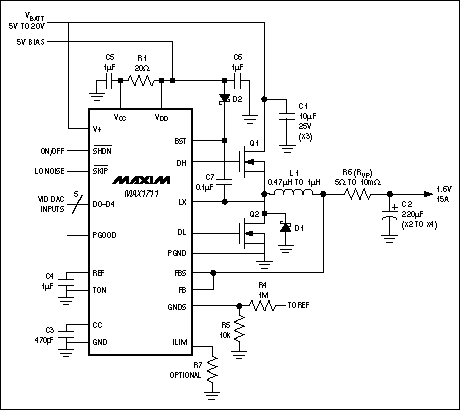
Figure 3. This efficient 15A regulated supply easily converts to a voltage-positioned design with the addition of three resistors: R4, R5, and R6 (RVP).
C1 = Ceramic Capacitor, C2 = Panasonic SP series: EEFUEOE221R.
*For continuous 15A load, use (2) IRF7811 or (2) IRF7805 due to thermal limitation of IR7809.
If RVP matches the filter capacitor's ESR, the output falls by the initial load-step drop (ESR × ILOAD), and remains at that level for as long as the load remains unchanged. Reducing the load causes the voltage level to rise by (ΔI × ESR). After a brief transient pulse from the last inductor discharge and before the controller's 100ns response (but within the allowed 7.5% limit), the dc level again remains at a level defined by the no-load voltage (1.62V in this case) minus ILOAD × RZ. See Figure 4.
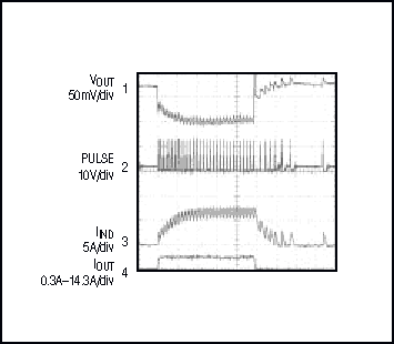
Figure 4. The step response of Figure 3's circuit illustrates the advantage of a voltage-positioned output.
Adding 5mΩ in series with the output reduces efficiency. However, it also reduces the CPU's operating voltage under heavy load, which lowers power dissipation and improves battery life. Compared with conventional (nonpositioned) regulators, a voltage-positioned design lowers the CPU dissipation by 1.38W and lowers the overall power consumption by 0.4W (Figures 5, 6).
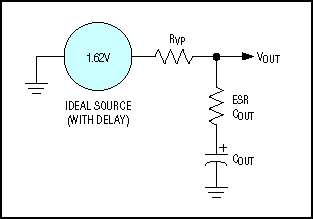
Figure 5. This simplified model illustrates the basics of voltage positioning. The ideal "square-wave" voltage response to a load step (Figure 2) occurs when RVP equals ESR (the effective series resistance of COUT).
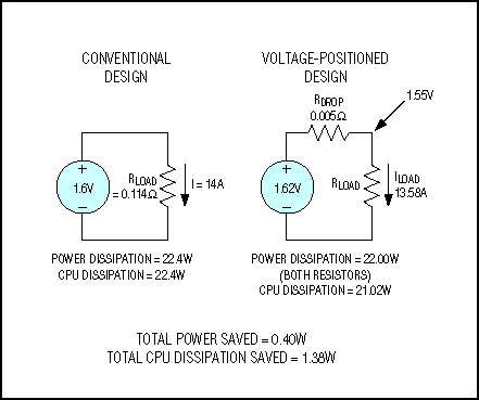
Figure 6. Despite added output resistance that reduces the conversion efficiency, a voltage-positioned design reduces power dissipation in the power supply and within the CPU.
Effective EfficiencyBecause this improvement comes at the expense of conversion efficiency, it may be helpful to propose a new term that compares a voltage-positioned circuit with a conventional (nonpositioned) one. This term, "effective efficiency," is the efficiency required in a nonvoltage-positioned design to equal the performance of a voltage-positioned design.
To determine the effective efficiency of a voltage-positioned regulator, first measure its efficiency in the conventional way [(VOUT × IOUT)/(VIN × IIN)], then model the load as a resistance for each efficiency data point (RLOAD = VOUT/IOUT). Next, calculate the output current for each RLOAD data point, using the nonpositioned output voltage (INP = VNP/RLOAD, where VNP = 1.6V in this case). Effective efficiency is then calculated at each INP data point, as the nonpositioned power output (VNP × INP) divided by the measured voltage-positioned power input (VOUT × IOUT). Note that an effective efficiency exceeding 100% is mathematically possible, but has yet to be achieved.
Figure 7 shows how dramatic this improvement can be for a typical CPU power supply. To match the benefits derived from voltage positioning, a conventional design at full load would need an efficiency improvement of nearly 8%.
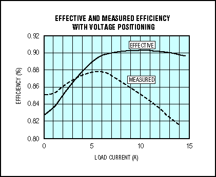
Figure 7. These plots show an 8% advantage for the voltage-positioned CPU power supply at full load. A conventional design would need 90% conversion efficiency to match the 82% efficiency of a voltage-positioned design delivering 14A.
欢迎分享,转载请注明来源:内存溢出

 微信扫一扫
微信扫一扫
 支付宝扫一扫
评论列表(0条)