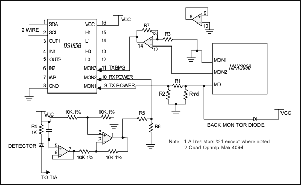

Figure 1.
TX Power originates at MAX3996 pin MD as a voltage representative of the back monitor diode's current. This voltage is 1.12V (±8%) and is independent of TX Power setting (back monitor diode current setting). R1 and R2 are chosen by design so that the voltage generated into the DS1858 complies with the TX Power dBm scale. For example, 0dBm is expected to generate a digital output of 2710h, according to SFF-8472. The voltage at DS1858(9) that would generate 2710h is 0.381V (since 2.5V generates FFFFh). This sets the nominal values of R2 (62k) and R1 (100k). The standard requires a 3dB accuracy. The errors are less than 13.5% or about 0.5dB (8% for the voltage at MD, and 0.5% FS or 3.5% for the DS1858, and 2% for the resistors).
RX Power is derived from average received power. The differential voltage is a measure of the detector current. It is converted to a single-ended voltage. For example, -10dBm is expected to generate a digital output of 3E8h, according to SFF-8472. The voltage at DS1858(10) that would generate 3E8h is 0.038V (since 2.5V generates FFFFh). If the average detector current into R4 is 100µA nominal then 100mV DC will be sensed by the instrumentation amp. The divider network to convert 100mV into 38mV consists of R5 = 10k and R6 = 6.2k. The standard requires a 3dB accuracy. The errors, excluding photodetector conversion, are less than 36% or 2dB (0.5% FS or 33% for the DS1858, and 3% for resistors and amplifier offset/bias errors). It is noteworthy that, in order to avoid significant common-mode errors, the 10k resistors have to be 0.1% with low temp co (50PPM/°C or less). This leaves room in the error budget for 1dB (+25%, -21%) to cover photodetector variation. If this is not sufficient for the particular photodetector used then a pot should be substituted for R4.
TX Bias originates within the MAX3996 (pin MON2) as a voltage proportional to bias current. For example, this voltage at 60mA is .66 V (±15%). R3 and R7 are chosen by design so that the voltage generated into the DS1858 complies with the bias current scale. For example, 60mA of bias current is expected to generate a digital output of 7530h, according to SFF-8472. The voltage at DS1858(11) that would generate 7530h is 1.14 (since 2.5V generates FFFFh). This sets the nominal values of R3 (10k) and R7 (7.15k). However because the standard requires a better than 10 % accuracy, a variable resistor or potentiometer is suggested for R3, such as the DS1804. Concluding RemarksThe preceding work shows that, for a given design, a discrete implementation of the internal calibration requirement is reasonably attainable within the allowable error budget of the SFF-8472 standard. Part-to-part variation was taken into account. By preprocessing the signal going into the DS1858 no loss of resolution occurs.
Other implementations using other laser drivers, will differ in detail only but will achieve similar results. Typically, two or three op amps and a small number of discrete components are adequate to achieve similar results.
欢迎分享,转载请注明来源:内存溢出

 微信扫一扫
微信扫一扫
 支付宝扫一扫
评论列表(0条)