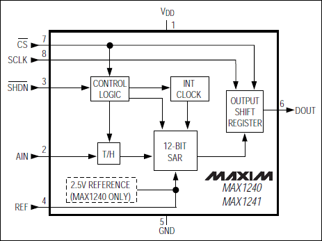
The MAX1240/MAX1241 low-power, 12-bit analog-to-digital converters (ADCs) are available in 8-pin packages. The MAX1240 operates with a single +2.7V to +3.6V supply, and the MAX1241 operates with a single +2.7V to +5.25V supply. Both devices feature a 7.5µs successive-approximaTIon ADC, a fast track/hold (1.5µs), an on-chip clock, and a high-speed, 3-wire serial interface.
Power consumpTIon is only 37mW (VDD = 3V) at the 73ksps maximum sampling speed. A 2µA shutdown mode reduces power at slower throughput rates.
The MAX1240 has an internal 2.5V reference, while the MAX1241 requires an external reference. The MAX1241 accepts signals from 0V to VREF
Excellent AC characterisTIcs and very low power combined with ease of use and small package size make these converters ideal for remote-sensor and data-acquisiTIon applications, or for other circuits with demanding power consumption and space requirements. The MAX1240/MAX1241 are available in 8-pin PDIP and SO packages.
关键特性
- +2.7V to +3.6V (MAX1240)
- +2.7V to +5.25V (MAX1241)
- 3mW (73ksps, MAX1241)
- 66µW (1ksps, MAX1241)
- 5µW (power-down mode)
应用/使用
电池供电应用
仪表
隔离型数据采集
便携式数据记录
过程控制

功能框图
欢迎分享,转载请注明来源:内存溢出

 微信扫一扫
微信扫一扫
 支付宝扫一扫
评论列表(0条)