Aperture Jitter Calculator for ADCs
Abstract: This applicaTIon note clarifies the operaTIon and applicaTIons of the Maxim Jitter Calculator provided as part of the ADC design tools. This document assumes that the reader has a basic understanding of terminology and concepts related to ADCs (For more informaTIon, see application note 641, "ADC and DAC Glossary.")
The Maxim Jitter Calculator is intended for use with ADCs that have a clock-based, input-sampling scheme (sample/track-and-hold (T/H) front-end) for acquisition of dynamic input signals. The calculator performs two different sets of calculations for ADC sampling-clock aperture jitter. The first calculation gives the theoretical maximum SNR limit imposed on ADC performance as a result of a specified value for aperture jitter (tJ, in seconds). The second calculation finds, the maximum allowable aperture jitter for a given resolution and frequency.
The SNR calculation assumes that the ADC in question is an "ideal" converter. In this context, ideal means that the ADC has both infinite resolution and no other limiting factors except the sampling aperture jitter. For a finite-resolution ADC, the maximum theoretical SNR will be lower than this theoretical maximum. When other limiting factors and imperfections present in a real design are also included, the SNR will fall even further. Therefore, these results are intended to represent an upper limit—not a realizable SNR result.
To derive the calculation, first start with a full-scale sinusoidal input signal defined as:
The rate of change (or slew rate) is then defined as:
By definition, the RMS value of a sinusoidal is the amplitude divided by √2:
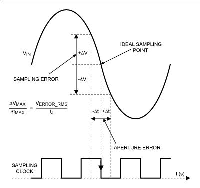
From this result, it follows that for any variation in the sampling instant (Δt), the input signal changes (ΔV) based on this slew rate. (See Figure 1.) 
Figure 1. Sampling voltage error as a result of aperture jitter.
Defining the worst-case variation in the sampling instant as the aperture jitter (tJ) and the corresponding worst-case RMS voltage error as VERROR_RMS, yields the combined expression:
Solving for VERROR_RMS:
The next step is to treat this sampling error as a noise source, and calculate the corresponding theoretical limit imposed by the aperture jitter on the SNR of the ADC. The RMS value of the full-scale sinusoidal input signal is:
It follows then, that the RMS input SNR, expressed in dB, is:
Simplifying the expression:
This is the equation used by the calculator to estimate the theoretical maximum SNR. The values for the input signal frequency, fIN (in Hz), and for the aperture jitter, tJ (in seconds), are user defined. Comparing this result to the theoretical maximum SNR imposed by quantization noise (and other effects) can help determine which will be the dominant limiting factor in the ADC performance.
To derive the maximum allowable aperture jitter for a given input frequency using a real ADC of fixed, finite resolution, a similar derivation is used.
First, as before, begin with a full-scale sinusoidal input signal defined as:
Also as before, the slew rate is defined as:
The worst case occurs at the maximum possible slew rate, which is the zero crossing (midscale for a unipolar ADC), where cos(2π × ƒIN × t) = 1. Therefore, the maximum rate of change can be defined as:
Typically, the assumption made to guarantee that the voltage error due to aperture jitter is tolerable, is to assure that it is smaller than VLSB/2. This means that based on the slew rate, the maximum change in voltage over time, tJ, must be less than VLSB/2. This yields the following expression:
Solving this expression for tJ:
Next, if VA is the amplitude, it represents half of the full-scale swing, or:
Combining the last two expressions:
Finally, simplifying the expression and collecting the terms results in:
Keep in mind that the calculator will return the value of tJ such that:
In this case, tJ is the maximum tolerable aperture jitter that can yield an idealized voltage error equal to VLSB/2. Good design practice, however, dictates that some margin should be built in to account for nonidealities present in any real design. Therefore, to ensure that the aperture jitter results in an error smaller than VLSB/2, specify an error budget for jitter well below the maximum limit presented by this calculation tool.
The two calculations which this tool can make will not agree. In the first calculation, an infinite-resolution ADC is assumed. The resulting calculation is the theoretical limitation to SNR from the aperture jitter only. The real SNR of a system with the given input frequency and aperture jitter will be lower than the calculated result due to all the nonideal effects neglected in this calculation. Only in cases where aperture jitter is the dominant limiting effect will real design expectations fall near this theoretical result.
In the second calculation, the ADC has a finite (integer), fixed resolution for a given input frequency. The calculation is then built on the assumption that the maximum allowable aperture jitter corresponds to a VLSB/2 error. A good design will target a value well below this upper limit.
欢迎分享,转载请注明来源:内存溢出

 微信扫一扫
微信扫一扫
 支付宝扫一扫
评论列表(0条)