Variable-reluctance (VR) sensors are preferred for industrial and automotive environments because they withstand mechanical vibration and high-temperature operation up to 300°C. In most applications, they sense a steel target that is part of a rotating assembly. Because the unprocessed signal amplitude is proportional to target speed, a sensor whose signal-processing circuitry is designed for high speed will cease to function as rotation slows.
Hall-effect sensors are preferred for lower speeds (several pulses per second), but they require that a magnet be attached to the rotating assembly, making them prone to failure when the magnet is broken or damaged. Neither type (VR or Hall-effect) offers fail-safe detection of the processed signal in the event of failure in the cable or sensor.
The circuit of Figure 1 is a fail-safe VR sensor suitable for low- to medium-speed operation. Comprising of L1, R1, and a quad RS-422/RS-485 receiver (IC1), it provides the complementary, independent output signals VOUT and Acitive-Low VOUT. Table 1 lists the resulting fail-safe modes. Supply voltage can be +10V, +12V, or the control system's +24V DC source.

Figure 1. This circuit provides a fail-safe, low-to-medium-speed, variable-reluctance sensor.
Table 1. Fail-safe modes (two cycles of VOUT or Active-Low VOUT)
*System remains functional in failure modes.
Coil L1 consists of 2600 turns of #32 magnet wire wound on a 0.800" steel bar of 0.200" diameter, with 0.125" protruding from the sensor face. A magnet attached to the back of the steel bar supplies necessary magnetic flux. The rotating target then causes a change in reluctance, hence a change in the amount of magnetic flux conducted, and therefore a change in the current induced in L1. R1 converts the L1 current to a time-varying voltage. This time varying voltage is applied to the inputs of IC1, whose wide input-voltage range (±25V), narrow input threshold (±0.2), and low input hysteresis (45mV typical) enable the VR sensor to operate at low speeds.
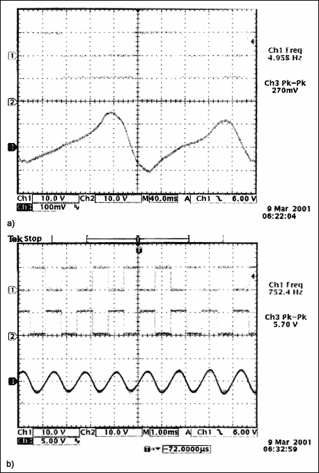
The separate and complementary outputs are derived from separate ESD-protected inputs. IC1 outputs Y1 and Y2 can source up to 10mA of current. They alternately switch the logic-rated n-channel MOSFETs Q1 and Q2, which in turn provide VOUT and Active-Low VOUT. An LDO voltage regulator (IC2) generates the +5VDC required by IC1. Figure 2 illustrates low- and medium-speed operation for the sensor.

Figure 2. These Figure 1 waveforms, produced by two targets 180° apart, illustrate low- and medium-speed operation: 4.9Hz at 2.4 revolutions/sec (a), and 752.4Hz at 376.2 revolutions/sec (b). Channel 1 is VOUT, Channel 2 is Acitve-Low VOUT, and Channel 3 is the voltage across R1.
For +5V-supply applications in which a microcontroller can be located close to the sensor, only L1, R1, and IC1 are required for a direct interface. For +3V applications, replace IC1 with a MAX3096 IC.
A similar version of this article appeared in the November 22, 2001 issue of EDN magazine.
欢迎分享,转载请注明来源:内存溢出

 微信扫一扫
微信扫一扫
 支付宝扫一扫
评论列表(0条)