
GENERAL DESCRIPTION
The HUSB238 is a highly integrated USB Power Delivery (PD) controller as sink role 。 The HUSB238 is compaTIble with USB PD3.0 V1.3 and Type C V1.4 and it can also support charge protocols such as Apple divider 3, BC1.2 SDP, CDP and DCP. The HUSB238 can be used in electronic devices that have legacy barrel connectors called Barrel Connector Replacement , BCR ) or USB micro B connectors 。 The applicaTIons can be wireless charger, IoT (Internet of Things) devices, drones, smart speakers, power tools, and other rechargeable devices. The HUSB238 is available in 3 mm x 3mm DFN 10L package and 3.9mm x 4 mm SOT33-6 package.
Figure 1. shows the photos of HUSB238 reference design board.
INTERFACE SPECIFICATIONS
Table 1. Reference Design Board Interface Specifications.

CIRCUIT CONNECTION
The circuit connection of HUSB238 reference design board with the PD power adapter and powered device is shown as below.
Figure 2. Circuit Connection of the HUSB238 ReferenceDesign Board
NOTES FOR THE REFERENCE DESIGN BOARD
The RDO of HUSB238 default factory setting is 20V3.25A. If the USB-C cable does not have an eMarker chip or the eMarker indicates the cable current rating being only 3A, the maximum current rating of source capability of the PD power adapter is only 3A and the PD power adapter fails to match the HUSB238. In this situation, the request current can be set to 3A(or smaller) by changing the external resistor RISET to 22kΩ (or smaller)。
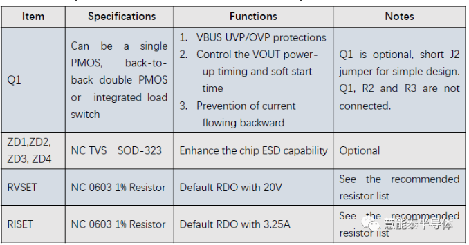
Table 2. Component Selection and Function Description
VOLTAGE AND CURRENT REQUEST PRINCIPLE
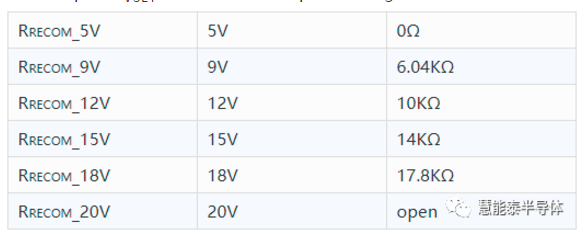
RECOMMEND RVSET & RISET RESISTOR VALUE LIST
The relationship of RVSET valueand the request voltage:
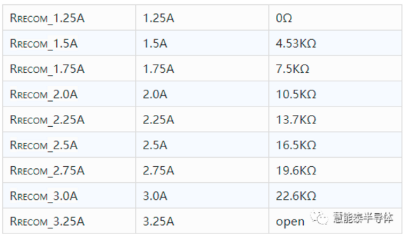
Therelationship of RISET valueand the request current:
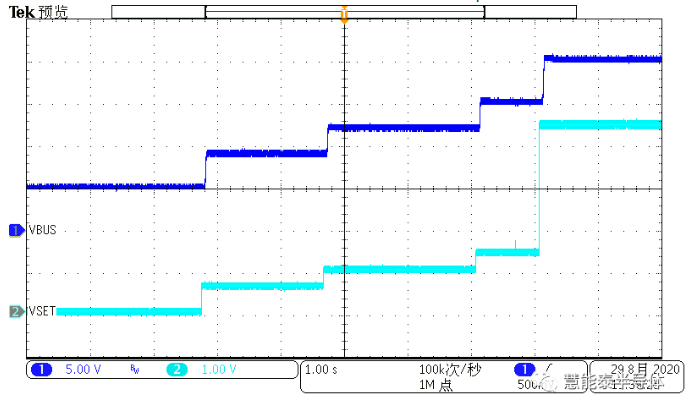
The target voltage and current are dynamically applied by changing the value of external resistors, which are connected to VSET and ISET pins.
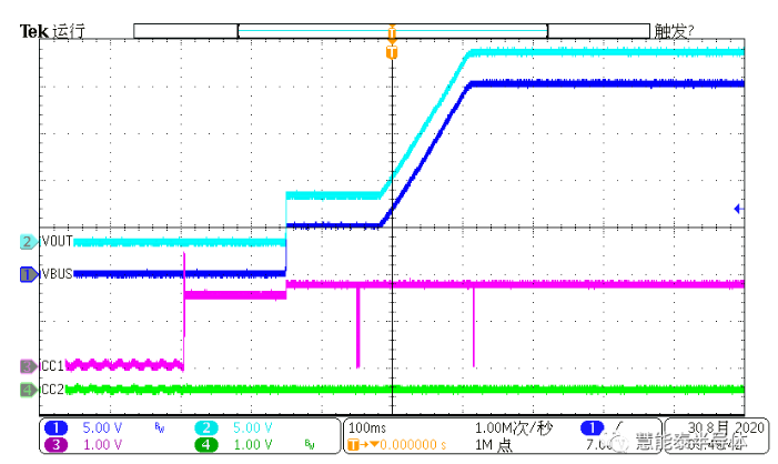
Figure 3. Dynamic Voltage Request Test Waveform
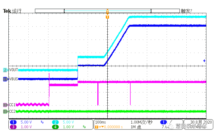
Figure 4. Start-up Waveform
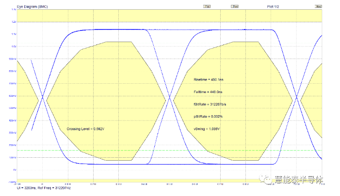
Figure 5. Eye Diagram of HUSB238
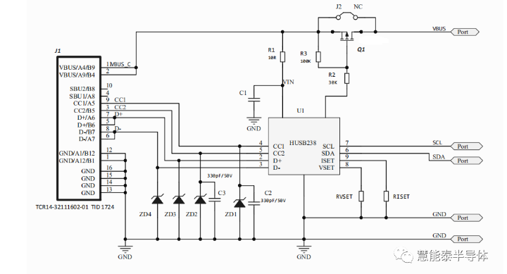
Figure 6. Schematic of HUSB238 ReferenceDesign Board
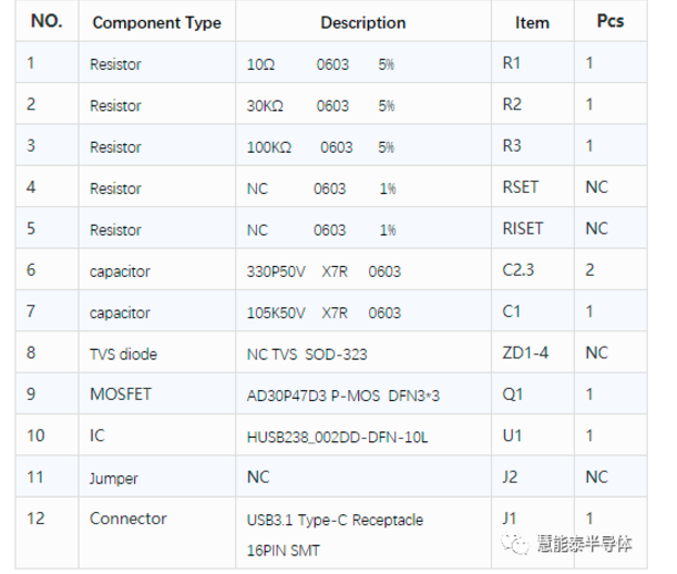
BOM LIST
Table 3. BOM of Reference Design Board
PCB LAYOUT
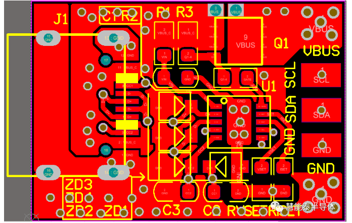
Figure 7. PCB Top View
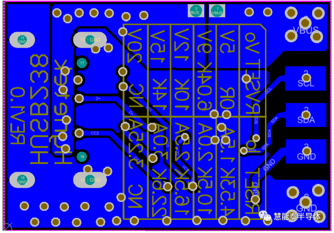
Figure 8. PCB Bottom View
欢迎分享,转载请注明来源:内存溢出

 微信扫一扫
微信扫一扫
 支付宝扫一扫
评论列表(0条)