Using the MAX4196 instrumentation amplifier (IA) as a pre-amplification circuit, adds a factor of 10V/V gain to the signal path enabling low output strain gauge sensors to be temperature compensated and calibrated. Complete circuits for high-gain amplification and temperature compensation of such sensors will be presented and discussed.
Pressure sensors and force sensors that use thin-film or thick-film (TF) strain gauge technology typically require signal amplification of several hundred volts per volt. The sensor signal must be compensated for changes in offset and span due to temperature changes.
The MAX1452 Precision Sensor Signal Conditioner provides all of the functions required for sensor bridge excitation (offset and span temperature compensation, and output offset adjustment with 16-bit trim resolutions). However, the MAX1452 design was optimized for piezo-resistive transducers (PRT), silicon micro-machined devices which typically require low signal gain due to their high bridge sensitivity.
The MAX1452 has a selectable gain range of 39-234V/V. PRT sensors can have full-scale (FS) output signal levels of 20-40 mV/V¹ and thus require a gain in the range of 42-83V/V when using 3V of bridge excitation voltage to produce an output voltage swing of 5V. TF sensors typically have much lower bridge sensitivity levels of 1.5 to 2.5 mV/V and thus require gains of 360-830V/V with a bridge excitation voltage of 4V to produce a 5V output swing.
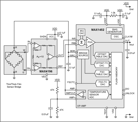
Using the MAX4196 instrumentation amplifier (IA) as a pre-amplification circuit adds a factor of 10V/V gain to the signal path enabling TF sensor calibration and temperature compensation with the MAX1452. A complete circuit for amplifying and temperature compensating a TF sensor using this architecture is shown in Figure 1.
Figure 1. The MAX4196 IA amplifies the sensor signal by a fixed gain of 10.
The MAX4196 was chosen² for its internally set fixed gain of 10 and requires no external components other than a bypass capacitor on the power supply. The op-amp in the MAX1452 is used to set an arbitrary mid-rail voltage of 2.5V to provide a reference signal to the MAX4196 REF input and to the MAX1452 INM input. The differential sensor signal is converted to a single-ended signal at the MAX4196 OUT pin with respect to the REF pin. The MAX1452 differential input is driven by this single-ended signal into the INP pin with respect to the INM input.
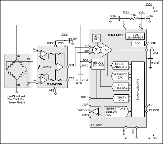
This provides a bipolar signal swing of the sensor signal about a zero-point set by the op-amp and resistor divider formed by the 47KΩ resistors. For sensors that have a positive offset at no-load and only swing in the positive output direction (such as typically found in weight sensor applications), the op-amp and resistor circuit can be eliminated by tying the MAX4196 REF and the MAX1452 INM pins directly to VSS. This is shown in Figure 2.
Figure 2. Unidirectional sensor connections.
The MAX1452 provides the bridge excitation for the sensor bridge. The excitation source is limited to 2mA in drive current capability when configured as a current source for PRT devices, but can deliver as much as 4mA of current when wired as a voltage excitation source (Pins BDR and ISRC connected together) and even higher currents with additional circuitry. With this current drive capability, TF sensors with bridge resistances as low as 1200Ω can be driven with excitation voltages of 4.5V. Since TF sensors typically have a very low temperature coefficient of resistance (TCR) and temperature coefficient of sensitivity (TCS) of the bridge, the excitation voltage does not require much compensation adjustment range and thus can be set to a value near the upper supply rail (typically VBDR = 4.5V). The higher the excitation voltage, the lower the required signal gains.
There are 16 gain settings for the MAX1452 that range from 39 to 234 in increments of 13. This range is expanded to 390 to 2340³ in increments of 130. The calibrated gain of the overall circuit is also a function of the bridge excitation voltage, VBDR, as shown in the following equation:
VOUT = BridgeOutput(mV/V) × VBDR(V) × GMAX4196(V/V) × GMAX1452(V/V)
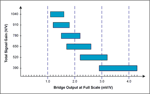
In order to have a continuous gain selection range, it is important that the fixed gain steps of the circuit overlap when using reasonable excitation voltages. A reasonable range of excitation voltages for TF sensors is 3.0-4.5V. The lower limit of 3.0V is imposed by consideration of system noise and the upper limit of 4.5V is imposed by the bridge excitation source requiring VBDR to be 0.5V below VDD for compliance or headroom for circuit operation. The overlapping gain selection ranges is shown graphically in Figure 3.
Figure 3. The overall selectable gain ranges provide overlap with various sensor outputs.
Since the MAX1452 modulates the bridge excitation voltage as a means to adjust the overall gain for compensation of span over temperature, it is important to look at this effect on the MAX4196 pre-amplifier. Typical TF sensors have very good TCS performance and may vary by only a few percent over a 100°C temperature range. This requires that the bridge excitation be varied by only a few percent, typically only Δ150mV, over the same temperature range in order to compensate the effect. This small change in VBDR will produce a small change in the common mode output voltage into the MAX4196. The MAX4196 provides a common-mode rejection of 88dB minimum over the operating range of -40°C to 85°C. At an overall system gain of 910V/V (worst-case calculations is at high gains) this translates into an output error signal of 0.1%.
An additional bonus of this increased gain architecture over those circuits that use a gain stage on the output of the MAX1452 is a significant improvement in noise performance. The MAX1452 programmable gain amplifier (PGA) is a switched capacitor architecture that generates a small, but significant, output noise. This noise level scales (non-linearly) with the PGA gain setting. Higher PGA gain settings produce a higher output noise. Placing the additional gain circuitry at the input to the MAX1452, and using the lower PGA gain settings can realize a high signal gain system.
Notes
¹Sensors wired in the Wheatstone bridge configuration are typically rated in millivolts of differential output signal per volt of bridge excitation voltage applied at the rated full-scale load of the sensor. Hence, a sensor rated at 2mV/V output at full-scale load will produce 8mV of differential output voltage when excited with 4V and full-scale load applied.
²The MAX4194 IA could be used equally well and provides a user-settable gain with the addition of an external gain setting resistor.
³Gains in excess of 1000 become dominated by system noise and are not suitable for general applications.
欢迎分享,转载请注明来源:内存溢出

 微信扫一扫
微信扫一扫
 支付宝扫一扫
评论列表(0条)