
本文介绍了LatTIceECP3 FPGA系列主要特性,LatTIceECP3-35简化方框图以及LatTIceECP3视频协议板主要特性,方框图和详细的电路图。
LatTIceECP3主要特性:
Higher Logic Density for Increased System Integration
• 17K to 149K LUTs
• 133 to 586 I/Os
Embedded SERDES
• 150 Mbps to 3.2 Gbps for Generic 8b10b, 10-bit SERDES, and 8-bit SERDES modes
• Data Rates 230 Mbps to 3.2 Gbps per channel for all other protocols
• Up to 16 channels per device: PCI Express, SONET/SDH, Ethernet (1GbE, SGMII, XAUI), CPRI, SMPTE 3G and Serial RapidIO
sysDSP™
• Fully cascadable slice architecture
• 12 to 160 slices for high performance multiply and accumulate
• Powerful 54-bit ALU operations
• Time Division Multiplexing MAC Sharing
• Rounding and truncation
• Each slice supports
–Half 36x36, two 18x18 or four 9x9 multipliers
–Advanced 18x36 MAC and 18x18 Multiply-Multiply-Accumulate (MMAC) operations
Flexible Memory Resources
• Up to 6.85Mbits sysMEM™ Embedded Block RAM (EBR)
• 36K to 303K bits distributed RAM
sysCLOCK Analog PLLs and DLLs
• Two DLLs and up to ten PLLs per device
Pre-Engineered Source Synchronous I/O
• DDR registers in I/O cells
• Dedicated read/write levelling functionality
• Dedicated gearing logic
• Source synchronous standards support
–ADC/DAC, 7:1 LVDS, XGMII
–High Speed ADC/DAC devices
• Dedicated DDR/DDR2/DDR3 memory with DQS support
• Optional Inter-Symbol Interference (ISI) correction on outputs
Programmable sysI/O™ Buffer Supports Wide Range of Interfaces
• On-chip termination
• Optional equalization filter on inputs
• LVTTL and LVCMOS 33/25/18/15/12
• SSTL 33/25/18/15 I, II
• HSTL15 I and HSTL18 I, II
• PCI and Differential HSTL, SSTL
• LVDS, Bus-LVDS, LVPECL, RSDS, MLVDS
Flexible Device Configuration
• Dedicated bank for configuration I/Os
• SPI boot flash interface
• Dual-boot images supported
• Slave SPI
• TransFR™ I/O for simple field updates
• Soft Error Detect embedded macro
System Level Support
• IEEE 1149.1 and IEEE 1532 compliant
• Reveal Logic Analyzer
• ORCAstra FPGA configuration utility
• On-chip oscillator for initialization & general use
• 1.2V core power supply
LatticeECP3™系列选择指引表: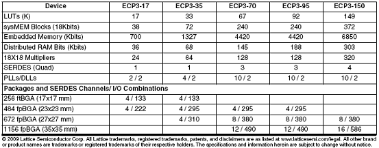
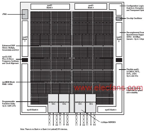
图1。LatticeECP3-35简化方框图(顶层)
LatticeECP3视频协议板
LatticeECP3 Video Protocol Board
The LatticeECP3™ FPGA family includes many features for video applications. For example, DisplayPort, SMPTE standards (SD-SDI, HD-SDI and 3G-SDI), DVB-ASI, DVI and HDMI can be implemented with 16 channels of embedded SERDES/PCS. 7:1 LVDS video interfaces like ChannelLink and CameraLink can be supported by the generic DDRX2 mode on the I/O pins. When configuring to TRLVDS mode, the I/O pins on banks 0 and 1 can also be used to receive the TMDS signals of DVI or HDMI video standard.
This user’s guide describes revision C of the LatticeECP3 Video Protocol Board featuring the LatticeECP3 LFE3-95E-7FN1156C FPGA device. The stand-alone evaluation PCB provides a functional platform for development and rapid prototyping of many different video applications. 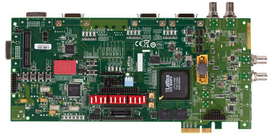
图2。LatticeECP3视频协议板外形图-Rev.C
主要特性:
• Video interfaces for interconnection to video standard equipment
• Allow the demonstration of SD/HD/3G-SDI, DisplayPort and PCI Express (x4) interfaces using SERDES channels
• High speed Mezzanine connector connected to SERDES channels for future expansion
• Allows the demonstration of LVDS video standards – ChannelLink and CameraLink
• Allows control of SERDES PCS registers using the Serial Client Interface (ORCAstra)
• Allows the demonstration of receiving TMDS signals using the DVI interface
• On-board Boot Flash with Serial SPI Flash memory device
• Shows interoperation with high performance DDR2 memory components
• Driver-based “run-time” device configuration capability via an ORCAstra or RS232 interface
• SMAs for external high-speed clock / PLL inputs
• Switches, LEDs and LCD display header for demo purposes
• Mictor connector for using Logic Analyzer in the debugging phase
• Input connection for lab-power supply
• Power connections and power sources
• ispVM™ programming support
• On-board and external reference clock sources
• Various high-speed layout structures
• User-defined input and output points
• Performance monitoring via test headers, LEDs and switches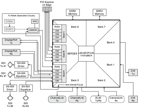
图3。LatticeECP3视频协议板-Rev. C功能框图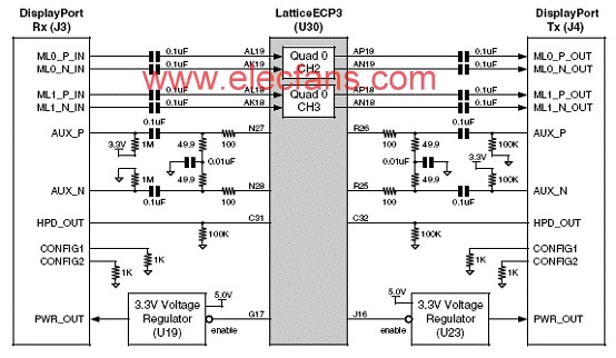
图4。DisplayPort 视频接口方框图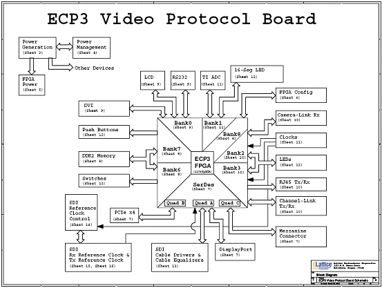
图5。LatticeECP3视频协议板方框图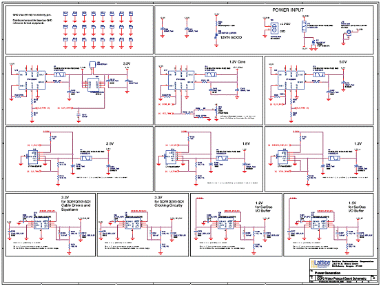
图6。LatticeECP3视频协议板电路图-电源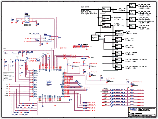
图7。LatticeECP3视频协议板电路图-电源管理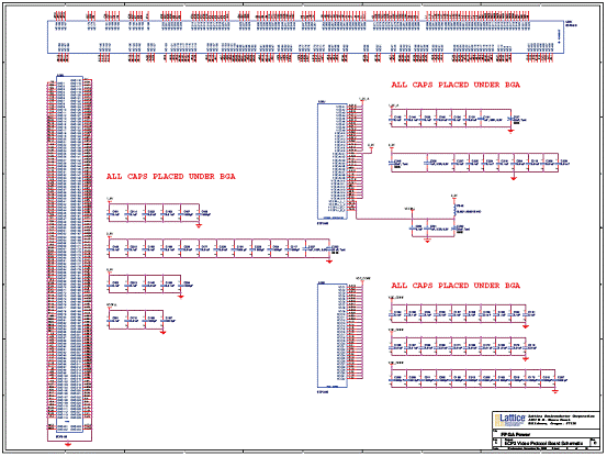
图8。LatticeECP3视频协议板电路图-FPGA电源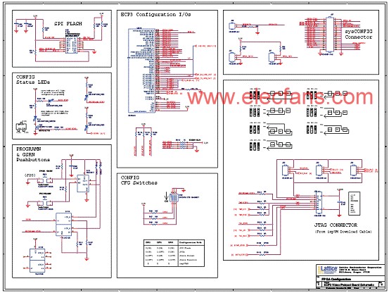
图9。LatticeECP3视频协议板电路图-FPGA配置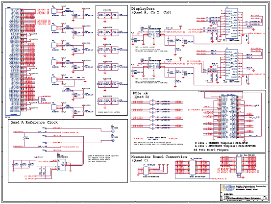
图10。LatticeECP3视频协议板电路图-SERDES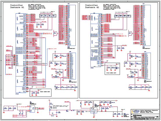
图11。LatticeECP3视频协议板电路图-DDR2存储器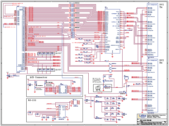
图12。LatticeECP3视频协议板电路图-DVVLCD/RS232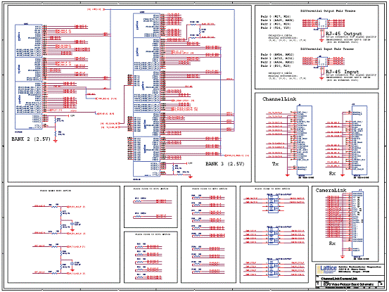
图13。LatticeECP3视频协议板电路图-通路/照相机连接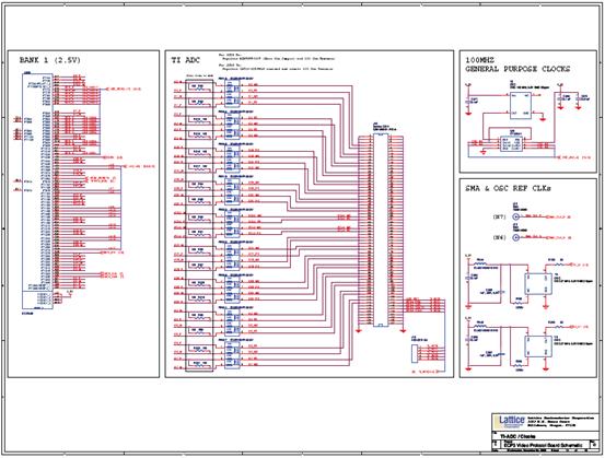
图14。LatticeECP3视频协议板电路图-TI ADC/CLOCK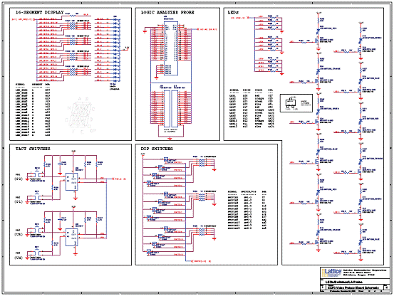
图15。LatticeECP3视频协议板电路图-LED/开关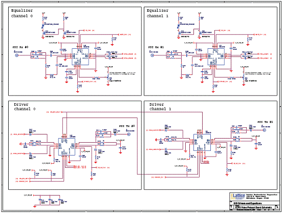
图16。LatticeECP3视频协议板电路图-SDI驱动/均衡器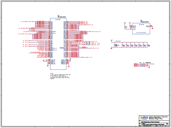
图17。LatticeECP3视频协议板电路图-SDI基准时钟控制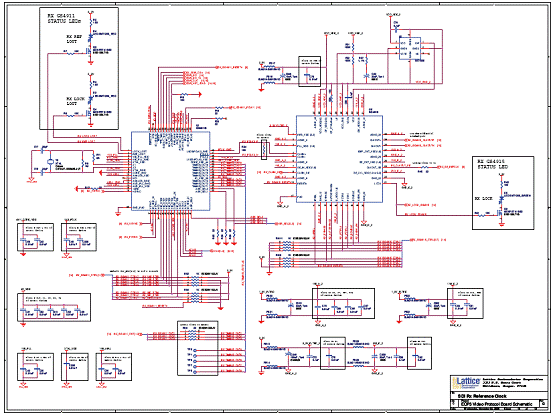
图18。LatticeECP3视频协议板电路图-SRI Rx基准时钟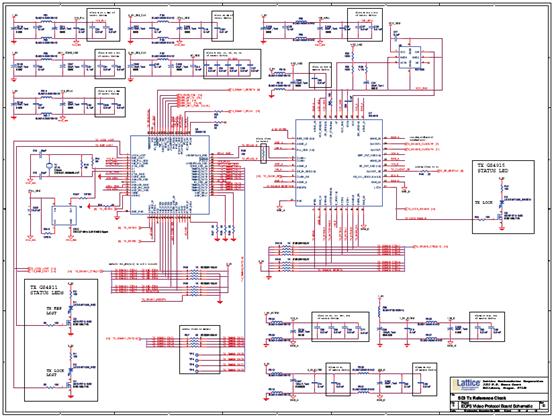
图19。LatticeECP3视频协议板电路图-SRI Tx基准时钟
欢迎分享,转载请注明来源:内存溢出

 微信扫一扫
微信扫一扫
 支付宝扫一扫
评论列表(0条)