The MAX7219/7221 is an 8-digit, 7-segment common-cathode mulTIplexed LED display driver which drives up to 40mA segment current while operaTIng from a 4V to 5.5V supply. This applicaTIon note discusses how the MAX7219/7221 can be used with external drive transistors for applications requiring higher peak segment currents and/or a higher drive voltage. LEDs using three or more LED dice per segment cannot be driven directly by the MAX7219/7221 from a 5V supply due to the multiple LED voltage drops.
The drivers shown in Figures 1 thru 4 interface a MAX7219/7221 operating at 4V to 5V to common anode displays operating at a higher segment current and/or drive voltage than the MAX7219/7221 can deliver. Eight instances of the low current cathode column driver, and eight instances of the high current anode digit driver are required.
The MAX7219/7221's PWM digital intensity control can still be used. The peak segment current, however, is now set by external current-limiting resistors in series with the LED cathodes instead of by resistor RSET.
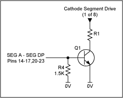
To use these drivers, choose R1 (see Figure 4) to set the desired peak LED segment current ISEG according to the driver supply voltage Vdriver and the LED forward voltage drop VLED:
IPEAK = (Vdriver - VLED - VCE(sat)Q1) / (R1 + RDS(on)Q2) ARate Q1 at segment current ISEG, and rate Q2 at digit current, which is 8 times ISEG.
Note that the display must be the common anode (CA) type to interface the drivers described here; the MAX7219/7221 directly drive common cathode (CC) displays, but these external drivers invert the digit/segment drive polarity. Digit DriversThe digit drive outputs of the MAX7219/7221 are power switches which go active low one at a time to turn a digit on, and high impedance when off.
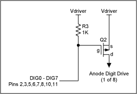
Three alternative digit drive circuits are suggested here. The simplest circuit (Figure 1) suits an application where a higher than 40mA segment current is desired, and yet the 4V-5V MAX7219/7221 supply voltage can be used to drive the LEDs. The active low MAX7219/7221 digit drive outputs directly drive logic level PFET Q2. Resistor R3 turns Q2 off when the digit output is high impedance. The supply Vdriver is the same supply as used by the MAX7219/7221.

Figure 1. Current boosting the digit drive while retaining a low voltage LED supply.
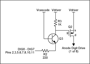
The circuit of Figure 2 includes a level shifter to allow a higher supply voltage than 5V to be used to drive the LEDs. Q3 operates as a common-base current switch, and sinks a collector current set by resistor R2 (about 5mA using Vcascode = 5V) when the digit drive output is low. This current in turn develops about 5V across the 1kΩ of R3 to provide a consistent gate drive to logic level PFET Q2, independent of the fluctuations of the supply Vdriver. Note, though, that the collector of Q3 can go no lower than VCE(sat)Q3 above it's emitter, which is at VBE below Vcascode.

Figure 2. Current boosting the digit drive using an LED supply 10V or higher.
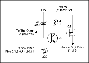
As R3 is dropping 5V, this places the lower limit for the supply Vdriver at about 10V if Vcascode is set to 5V. 5V was picked as a convenient voltage for Vcascode because it's likely to be the supply for the MAX7219/7221. However Vcascode can be set to a lower voltage, such as 2V, by simply dropping the 5V supply through a zener diode (Figure 3). Only one zener diode is needed to serve all the digit drivers.

Figure 3. Current boosting the digit drive using an LED supply below 10V. Segment DriversThe MAX7219/7221 segment drive outputs are current sources, which drive a constant current set by resistor RSET connected to the ISET pin of the MAX7219/7221. The maximum segment current is 40mA. To drive a higher segment current, external transistors and segment current limiting resistors are needed (Figure 4).

Figure 4. Current boosting the segment drive.
By setting the MAX7219/7221 segment drive current source correctly, a base current limiting resistor is not required for the segment drive switch Q1. The segment drive current can be set to be an appropriate value using RSET to turn Q1 on hard. Resistor R4 is needed to ensure Q1 turns off reasonably fast at the end of each digit's multiplex cycle. An RSET value around 150kΩ is a good starting point.
欢迎分享,转载请注明来源:内存溢出

 微信扫一扫
微信扫一扫
 支付宝扫一扫
评论列表(0条)