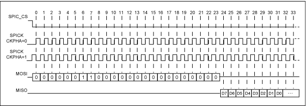
SPI™ Serial EEPROM InterfaceThe SPI interface is a four-signal serial interface that allows configuraTIon of the DS33Z11/DS33Z44 through an external serial EEPROM. When the mode-control pins are set properly (HWMODE = 0, MODEC1 = 1, and MODEC0 = 0), the DS33Z11/DS33Z44 acts as an SPI master and reads the data from the serial EEPROM. The MOSI (master out, slave in) and MISO (master in, slave out) are for data flow, while the SPICK and active-low SPI_CS signals control access to the EEPROM. The CKPHA pin can be used to configure the sampling and update edges of the MISO and MOSI signals. The MOSI data can be output on the rising or falling edge of SPICK. The MISO data can be sampled on rising or falling edge of SPICK. The SPICK operates at a frequency of 8.33MHz, which is generated by dividing down the external 100MHz SYSCLKI signal. SPI EEPROM Programming SequenceBecause the DS33Z11/DS33Z44 uses a fixed SPI memory-read instruction, the EEPROM used in conjunction with the DS33Z11/DS33Z44 must be a 16kB (2048 x 8) SPI serial EEPROM. SPI serial EEPROMs that have smaller memory sizes use a different memory-read instruction that is incompatible. The reading sequence begins after the initial power-on reset or the rising edge of the active-low RST pin. The DS33Z11/DS33Z44 initiates a memory read by bringing the SPI_active-low CS signal low, and then clocking out the SPI data-read instruction 0b00000011 on the MOSI data line. This is followed up by the 16-bit binary address for location 0x0000. The data is then read sequentially on the MISO data line. The SPI_active-low CS remains low until all of the data is read and latched by the DS33Z11/DS33Z44. The length of data read from the EEPROM will depend on whether the DS33Z11 or DS33Z44 is connected to the EEPROM. Figure 1 shows the functional timing of the DS33Z11/DS33Z44 reading from the EEPROM. Table 1 provides the memory map for the DS33Z11, while Table 2 provides the memory map for the DS33Z44.

Figure 1. SPI master functional timing.
Table 1. DS33Z11 EEPROM Program Memory Map
Table 2. DS33Z44 EEPROM Program Memory Map
The Ethernet MAC specific registers are addressed indirectly and require multiple write instructions when configured using a µP in parallel port mode. Because it is not possible to directly map these indirect registers into the EEPROM memory, a special programming sequence is required when using the SPI serial EEPROM programming mode. The indirect MAC registers are programmed using separate 7-byte records located at the end of the EEPROM memory map. Four MAC registers can be programmed in EEPROM mode: SU.MACCR, SU.MACMIID, SU.MACMIIA, and SU.MACFCR. The remaining indirect MAC registers should not need to be programmed, as they are MAC-status or status-configuration registers that require no initialization.
The 7-byte records essentially emulate the µP write sequence needed when accessing the indirect MAC registers. The first four bytes in the record contain the 32-bit data that will be written to the Ethernet MAC data 0 through 3 registers (SU.MACWD0-SU.MACWD3). The next two bytes in the record contain the 16-bit address that will be written to the Ethernet MAC address low and high registers (SU.MACAWL - SU.MACAWH). Finally, the remaining byte will be written to the Ethernet MAC read/write command status register (SU.MACRWC), which will trigger the actual write of the data to the specified address. One difference in the number of indirect writes allowed is seen in the DS33Z44. Ethernet interface 1 of the DS33Z44 has four records available for indirect writes, just like the DS33Z11. However, the remaining three Ethernet interfaces are only allowed two records for indirect writes. The reason for this is that there is only one MDIO port to manage external PHY(s), and it is controlled through MAC 1. Thus, the SU.MACMIID and SU.MACMIIA writes are only valid from the MAC 1 register set. To control more than one external PHY through the MDIO port of MAC 1, all of the PHYs MDIO ports must be tied togther and configured with the same external address.
An example is shown in Table 3, where the value 0x1018000C is written to the Ethernet MAC control register (SU.MACCR), which has an indirect address of 0x0000. For further assistance with the DS33Z11/DS33Z44 using the SPI serial EEPROM-programming mode, please use the links found in the following References section.
Table 3. Example of a DS33Z11 Indirect write
For more information about the DS33Z11 or DS33Z44, please consult the appropriate data sheet available at www.maxim-ic.com/telecom.
SPI is a trademark of Motorola, Inc.
欢迎分享,转载请注明来源:内存溢出

 微信扫一扫
微信扫一扫
 支付宝扫一扫
评论列表(0条)