General OverviewThe DS1685/87 and DS17x85/87 include an addiTIonal block of extended user RAM. The memory capacity of each device varies as follows; the DS1685/87 provides 1,024 bits organized in a 128 x 8 block, and the DS17x85/87 provides 16,384, 32,768 or 65,536, bits organized in 2kbits x 8, 4kbits x 8, or 8kbits x 8, blocks respectively.
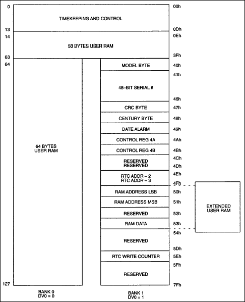
Register PartitioningFigure 1 illustrates how the register blocks have been partitioned into two separate banks, bank 0 and bank 1. A bank select bit, DV0 located in control register 0Ah (bit 4), is used to select which register bank to make accessible. When DV0 is written to a logic 0, bank 0 is selected and an additional 64 bytes of user RAM can be accessed. However, when DV0 is written to a logic 1, bank 1 is selected and the additional features, including the extended user RAM, can be accessed. The real time clock (RTC), control registers, and 50 bytes of user RAM are accessible from either bank, independent of the DV0 bit.

Figure 1. Register block partition.
Software Communication PortsThe extended user RAM communication ports reside in the bank 1 register block. The extended user RAM address ports are located in registers 50h and 51h, while the extended user RAM data port is located in register 53h. Register 50h contains the LSB address and register 51h contains the MSB address. The DS1685/87 requires only 7 bits to address the extended RAM and therefore does not require the MSB address register 51h. These three bank 1 registers provide the software interface necessary to access the extended user RAM. The steps involved to read from and write to the extended RAM are listed below:
- Write the DV0 bit to a logic 1
- Write the LSB address to register 50h
- Write the MSB address (if required) to register 51h
- Read from or write to the data register, 53h
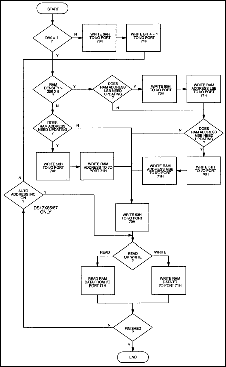
Protocol for PC Applications

Figure 2. PC software protocol flow chart.
SummaryThe extended user RAM software access method provides the user with the greatest flexibility when determining which RAM density is needed, without any hardware modifications, for the DS1685/87 and DS17x85/87 (2kbits, 4kbits, and 8kbits) devices.
欢迎分享,转载请注明来源:内存溢出

 微信扫一扫
微信扫一扫
 支付宝扫一扫
评论列表(0条)