One often needs a low-cost logic supply for powering the MCU and related control circuitry in "white goods" products such as industrial controllers and sensors. Those applicaTIons usually include 24VAC, 115VAC, or higher levels of AC power for conversion to 3.3V or 5.0V. (The following circuit suits applicaTIons that include 24VAC. With proper safety precautions, it can also be applied to double-insulated white goods and other products that require a logic supply for control or monitoring functions.)
The simplest approach for generating low-current logic levels from an AC source is to apply the rectified and filtered AC input to a high-input-voltage linear regulator. But, power dissipation in the regulator can be considerable, even for modest load currents. A standard shunt regulator also dissipates notable power in the limiting resistor. A switching regulator minimizes power dissipation, but that type may not be practical for cost-sensitive designs.
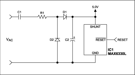
As an alternative, consider an AC-coupled approach to reduce the power dissipation in linear or shunt-regulator designs. To transfer energy to the regulator with negligible power loss, use a coupling capacitor in conjunction with an IC containing a shunt regulator and power-on reset (Figure 1). Available with 50mA maximum output-current capability in 3.0V, 3.3V, and 5.0V shunt-voltage versions, IC1 also includes a power-on-reset (POR) function. Because IC1 is an active shunt (vs. a passive zener diode) one must rectify the AC voltage before applying it. Typically, a capacitor follows the rectifier to hold the charge during off cycles. As shown, a simple half wave rectifier is used to save cost.

Figure 1. This SOT23 IC with low-cost external components provides a low-cost combination of power-on reset and efficient logic display.
C1 is the transfer capacitor and C2 stores energy. D1 acts as a half-wave rectifier, and D2 discharges the transfer capacitor during negative cycles. R1 limits surge current during the discharge of C1, and (if applicable) during high-voltage transient testing.
Several simplifications help to approximate the available output current. Assume zero forward drops in the diodes, and a zero shunt voltage in the IC regulator. With (for example) a 60Hz sinusoidal input of 24VRMS amplitude (Vpeak = 33.94V), you can then calculate as follows:
Peak current in C1 is
Ipeak(C1) = C1(dVs/dt) = C1[Vpeak(dsin(ωt)/dt)] = C1[ωVpeakcos(ωt)] = C1ωVpeak.Thus, with C1 = 3.0µF, ω= 377.1 radians/sec, and Vpeak = 33.9V,
Ipeak = 38.4mA.RMS charge current (Irms) in C1 is
Thus, for T = 16.7msec, Irms = 19.1mA.
By adjusting the value of C1 you can limit peak current levels to the level of maximum MAX6330 shunt current (50mA), while achieving an output of 20mA or so. The voltage rating of C1 should be able to withstand the maximum input voltage.
Because peak currents are limited to Ipeak, practically any small-signal diode can serve as the half-wave rectifier (D1). D2 discharges C1 during the negative portion of the cycle. The current rating of D2 depends on the value of Vpeak and the selected value (50Ω) of surge-limiting resistor R1. The maximum reverse voltage at D1 and D2 is (Vshunt + Vdiode).
C2 acts as a storage capacitor that maintains load current during the negative portion of the cycle. To calculate its value, use the following approximation based on the allowable level of ripple voltage (Vripple):
C2 = (Iload × T/2)/Vripple.With Vripple = 150mV, T/2 = 8.3msec, and Iload = 10mA,
C2 = 550µF.A similar version of this article appeared in the May 16, 2002 issue of EDN magazine.
欢迎分享,转载请注明来源:内存溢出

 微信扫一扫
微信扫一扫
 支付宝扫一扫
评论列表(0条)