
To be successful, the next generation of portable products, such as personal communicators and digital assistants, will have to provide at least 12 hours of operation between battery charges. Most of the progress toward this 12-hour goal must come from RF, computer, and battery technology, because power-supply performance is approaching a limit. Typical conversion efficiencies already exceed 95%. Still, the power supply must squeeze the battery for all it's worth. A key element in this task, especially at the low output voltages that future microprocessor and memory chips will need, is the synchronous rectifier.
A synchronous rectifier is an electronic switch that improves power-conversion efficiency by placing a low-resistance conduction path across the diode rectifier in a switch-mode regulator. MOSFETs usually serve this purpose, but bipolar transistors and other semiconductor switches are also suitable.
The forward-voltage drop across a switch-mode rectifier is in series with the output voltage, so losses in this rectifier determine efficiency almost entirely. As supply voltages ratchet downward, the design of rectifiers requires more attention, because the devices' forward-voltage drop constitutes an increasing fraction of the output voltage. The race to new voltage levels proceeds in jumps, as each major µP manufacturer brings successive fabrication processes on line. Currently, rumors for soon-to-be-released µPs indicate a VCC of 1.1V.
If you think low-voltage supplies are still a long way off, consider that the Joint Electronic Device Engineering Council (JEDEC) has drafted an interface standard for 2.5V low-voltage supplies. Beyond that, a standard is needed for the 1.5V supply used to terminate high-speed data buses, such as the 66MHz Gunning Transceiver Logic bus. The bus, which Bill Gunning at Xerox invented, comprises 144 or more open-drain transistor drivers, each with a 50w resistive pullup to the 1.5V source. Other low-voltage data buses include Rambus, Futurebus, HSTL, and CTT. So, a low-voltage-supply bus will probably soon come your way.
Even at 3.3V, rectifier loss is significant. For step-down regulators with a 3.3V output and a 12V battery input, the 0.4V forward voltage of a Schottky diode represents a typical efficiency penalty of about 12%, aside from other loss mechanisms. The losses are not as bad at lower input voltages, because the rectifier has a lower duty cycle and thus a shorter conduction time. However, the Schottky rectifier's forward drop is usually the dominant loss mechanism.
Figure 1 shows the efficiency gain using a synchronous rectifier. For an input voltage of 7.2V and an output of 3.3V, a synchronous rectifier improves on the Schottky diode rectifier's efficiency by around 4%. Figure 1 also shows that, as output voltage decreases, the synchronous rectifier provides even larger gains in efficiency.
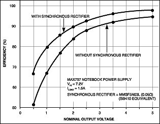
Figure 1. Data based on a high-performance buck switch-mode regulator and powered from a standard 7.2V notebook-computer battery shows that the synchronous rectifier has little effect on efficiency at 5V, but offers significant improvements at 3.3V and below. Diode versus Synchronous Rectifiers In the absence of a parallel synchronous rectifier, the drop across the rectifier diode in a switching regulator (Figure 2a) causes an efficiency loss that worsens as the output voltage falls. The Schottky diode in Figure 2a's simple buck converter clamps the switching node, the inductor's swinging terminal, as the inductor discharges.
In the synchronous-rectifier version of Figure 2b, a large N-channel MOSFET switch replaces the diode and forms a half-bridge configuration that clamps the switching node to -0.1V or less. The diode in Figure 2a clamps this node to -0.35V. Intuitively, losses in either type of rectifier increase with reduced output voltage. At VIN2VOUT, the rectifier voltage drop is in series with the load voltage for about half the switching period. As the output voltage falls, power lost in the rectifier becomes a greater fraction of the load power.
The basic trade-off between using diode or MOSFET rectifiers is whether the power needed to drive the MOSFET gate cancels the efficiency gained from a reduced forward-voltage drop. The synchronous rectifier's efficiency gain depends strongly on load current, battery voltage, output voltage, switching frequency, and other application parameters (see the tables in Figure 2). Higher battery voltage and lighter load current enhance the value of a synchronous rectifier. The duty factor, which equals 1-D, where D equals ton/(ton+toff), for the main switch, increases with the battery voltage. Also, the forward drop decreases with the load current.
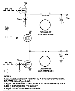
Figure 2. A synchronous rectifier simply replaces the Schottky diode in (a) with a low RDS(ON)MOSFET (b). This lower-resistance conduction path improves efficiency for a 5V to 3.3V 3A converter to around 3% to 4%.
The gate-drive signal is a key factor in calculating a synchronous rectifier's efficiency gain. For example, you can reduce gate loss by using a gate drive of 5V (as for logic-level MOSFETs) instead of the input (battery) voltage. You can simply supply the gate drive from a 5V linear regulator powered from the battery. Better yet, you can bootstrap the gate driver's power-supply rails from the regulator's output voltage. (This approach adds complexity in the form of a bypass switch for the initial power-up.) Also, you must weigh the lower loss associated with reduced gate voltage against the higher RDS(ON) resulting from a less-enhanced MOSFET.
When comparing diode and synchronous rectifiers, note that the synchronous rectifier MOSFET doesn't always replace the usual Schottky diode. To prevent switching overlap of the high-side and low-side MOSFETs that might cause destructive cross-conduction currents, most switching regulators include a dead-time delay. The synchronous rectifier MOSFET contains an integral, parasitic body diode that can act as a clamp and catches the negative inductor voltage swing during this dead time. However, this body diode is lossy, is slow to turn off, and can cause a 1% to 2% efficiency drop.
Therefore, designers interested in squeezing the last percent of efficiency out of their power supply place a Schottky diode in parallel with the synchronous rectifier MOSFET. This diode conducts only during the dead time. A Schottky diode in parallel with the silicon body diode turns on at a lower voltage, ensuring that the body diode never conducts. Generally, a Schottky diode used in this way can be smaller and cheaper than the type the simple buck circuit requires, because the average diode current is low. (Schottky diodes usually have peak current ratings much greater than their DC current ratings.) It's important to note that conduction losses during the dead time can become significant at high switching frequencies. For example, in a 300kHz converter with a 100nsec dead time, the extra power dissipated is equal to ILOAD x VFWD x td x f = 6 mW (where f is the switching frequency and td is the dead time) for a 2.5V, 1W supply, which represents an efficiency loss of about 0.5%.
Light-load efficiency is a key parameter for mobile applications in which the computer spends a long time in a nearly dormant suspend mode. For the buck-type switch-mode regulators often used in portable equipment, the synchronous rectifier's control circuit has a strong influence on light-load efficiency and noise performance. The key issue for light-load or no-load conditions is the timing of the MOSFET's turn-off signal.
When load current is light, the inductor current discharges to zero, becoming discontinuous or reversing direction. You have at least three options in dealing with this problem. You can continue to hold the synchronous switch on until the beginning of the next cycle, allowing the inductor to reverse. You can completely disable the synchronous rectifier at light loads. Or, you can sense the inductor current's zero crossing and shut off the synchronous rectifier on a cycle-by-cycle basis. Each approach involves a trade-off in different areas.
In the past, the option that designers widely used was holding the inductor switch on until the beginning of the next cycle (Figure 3a), which requires driving the MOSFET gates with complementary waveforms. This approach produces lower noise and allows a simple control scheme: The gate-drive signal is simply an inverted, opposite-phase version of the drive signal for the high-side switch. Noise is lower for two reasons, both of which relate to the continuous inductor current. First, the absence of pulse skipping ensures a constant switching frequency, regardless of load. A constant, fundamental switching frequency ensures that output ripple and EMI at the harmonic frequencies won't cause havoc in the IF bands of an audio or radio system. Second, this approach eliminates the dead time during which a resonant-tank circuit comprising the inductor and stray capacitance at the switching node can introduce ringing.
The drawback of letting the inductor current reverse is that the synchronous rectifier pulls current from the output. The circuit replaces this lost output energy during the next half cycle. However, at the beginning of the cycle when the high-side switch turns on, the circuit transfers the inductor energy stored during the earlier current reversal to the input-bypass capacitor.
This action resembles perpetual motion, in which energy shuttles between the input and output capacitors. Unfortunately, friction spoils all perpetual-motion schemes. In this case, the friction consists of switching and I2R losses. As energy shuttles back and forth, the circuit dissipates power in all its tiny parasitic resistances and switching inefficiencies. Thus, additional energy is necessary to maintain the shuttling action. The most obvious consequence is a high no-load supply current of typically 5mA for the 2.5V, 1W circuit.
The second option, turning off the synchronous rectifier entirely at light loads, offers simplicity and low quiescent supply current. You usually implement this method in conjunction with a pulse-skipping operation, governed by a light-load pulse-frequency-modulation (PFM) control scheme. Whenever the circuit goes into its light-load pulse-skipping mode, the circuit disables the synchronous rectifier that lets an accompanying parallel Schottky diode do all the work. Disabling the synchronous rectifier prevents the reversal of inductor current, and the problem of shuttling energy back and forth does not arise.
The final option, sensing the inductor current's zero crossing and quickly latching the synchronous rectifier off, turns off the synchronous rectifier on a cycle-by-cycle basis (Figure 3b). This method provides the highest light-load efficiency, because the synchronous rectifier does its job without allowing the inductor current to reverse. But, to be effective, the switching-regulator IC's current-sense amplifier that monitors the inductor current must combine high speed with low power consumption.
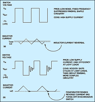
Figure 3. Allowing the inductor current to reverse provides the low-noise characteristics important to wireless computers with RF data links but degrades the light-load efficiency (a). Turning off the synchronous switch at light loads results in a ringing waveform similar to that of a diode rectifier (b).
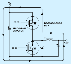
Figure 4. If you use the complementary gate-drive approach and the output is loaded lightly, the inductor current reverses during the synchronous rectifier's on time and the next half cycle begins with current flowing backward through the high-side MOSFET (MOSFETs are bidirectional). During the switching dead time, current flows through the parasitic diode.
A logic-control input can shift the synchronous-rectifier operation from the complementary-drive option to the off-at-zero option (Figure 5). When low, *SKIP* allows normal operation: The circuit employs pulse-width modulation (PWM) for heavy loads and automatically switches to a low-quiescent-current pulse-skipping mode for light loads. When high, *SKIP* forces the IC to a low-noise fixed-frequency PWM mode, regardless of the load. Also, applying a high level to *SKIP* disables the IC's zero-crossing detector, allowing the inductor current to reverse direction, which suppresses the parasitic resonant LC tank circuit.
Such control comes in handy for computers with built-in radios. When the radio is not in use and the host system goes from run mode to suspend mode, the power supply automatically assumes its light-load pulse-skipping mode to save power. If the RF transceiver is turned on, a logic signal forces the supply to a low-noise mode that maintains quiet operation, regardless of output load.
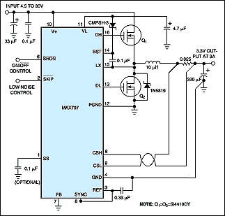
Figure 5. This N-channel buck regulator has a low-noise logic-control input that adjusts the synchronous rectifier's timing on the fly.
Another issue related to a synchronous rectifier's gate-drive timing is the cross regulation of multiple outputs that you can obtain using flyback windings. Many designers know that placing an extra winding or a coupled inductor on a buck regulator's inductor core can provide an auxiliary output voltage for the cost of a diode, a capacitor, and a few pennies' worth of wire (Figure 6). However, fewer designers know that a synchronous rectifier can help to regulate this output.
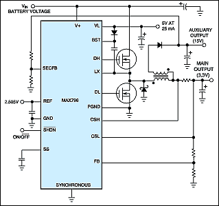
Normally, the coupled-inductor flyback trick in Figure 6 stores energy in the core when the high-side switch is on and discharges some of it through the secondary winding to an auxiliary 15V output when the synchronous rectifier's low-side switch is on. During discharge, the voltage across the primary is equal to VOUT+VSAT, where VOUT is the main output and VSAT is the synchronous rectifier's saturation voltage. Therefore, the secondary output voltage equals the primary output times the turns ratio.
Unfortunately, if the synchronous rectifier turns off at zero current and the primary load is light or nonexistent, the 15V output sags to ground, because the core stores no energy at this time. If the synchronous rectifier remains on, the primary current can reverse and let the transformer operate in the forward mode, providing a theoretically infinite output-current capability that prevents the 15V output from sagging. Unfortunately, quiescent supply current suffers a great deal.
However, the circuit in Figure 6 achieves excellent cross regulation with no penalty in quiescent supply current. A second, extra feedback loop senses the 15V output. If this output is in regulation, the synchronous rectifier turns off at zero current as usual. If the output drops below 13V, the synchronous rectifier remains on for an extra microsecond after the primary current reaches zero. Thus, the 15V output can deliver hundreds of milliamps even with no load on the main 5V output. This scheme also provides a better 15V-load capability at low values of VIN-VOUT, which becomes important as the battery voltage declines with discharge. Secondary-Side Synchronous Rectifiers Multiple synchronous rectifiers on the secondary windings can replace the usual high-voltage rectifier diodes in multiple-output nonisolated applications (Figure 7). This substitution can dramatically improve load regulation on the auxiliary outputs and often eliminates the need for linear regulators, which you would otherwise add to increase the output accuracy. You must select a MOSFET with a breakdown rating high enough to withstand the flyback voltage, which can be much higher than the battery voltage. Tying the gates of the secondary-side MOSFETs directly to the gate of the main synchronous MOSFET (the DL terminal) provides the necessary gate drive.
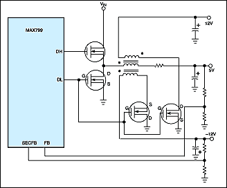
Figure 7. Coupled-inductor secondary outputs can benefit from synchronous rectification. To accommodate negative auxiliary outputs, simply swap the secondary-side MOSFET's drain and source terminals. (For clarity, this simplified schematic omits most of the ancillary components needed to make the switching regulator work.)
Another neat trick enables a synchronous rectifier to provide gate drive for the high-side switching MOSFET. Tapping the external switching node to generate a gate-drive signal higher than the battery voltage enables the use of N-channel MOSFETs for both switches in a synchronous-rectifier buck converter. Compared to P-channel types, N-channel MOSFETs have many advantages, because their superior carrier mobility confers a near 2:1 improvement in gate capacitance and on-resistance.
A flying-capacitor boost circuit provides the high-side gate drive (Figure 8). The flying capacitor is in parallel with the high-side MOSFET's gate-source terminals. The circuit alternatively charges this capacitor from an external 5V supply through the diode and places the capacitor in parallel with the high-side MOSFET's gate-source terminals. The charged capacitor then acts as supply voltage for the internal gate-drive inverter, which is comparable to several 74HC04 sections in parallel. Biased by the switching node, the inverter's negative rail rides on the power-switching waveform at the LX terminal.
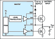
Figure 8. Driven by the switching node (the left end of the inductor), the capacitor between BST and LX provides an elevated supply rail for the upper gate-drive inverter.
The synchronous rectifier is indispensable to Figure 8's gate-drive boost supply. Without this low-side switch, you can't guarantee that the circuit will start at initial power-up. When power is first applied, the low-side MOSFET forces the switching node to 0V and charges the boost capacitor to 5V. On the second half-cycle, the gate driver's DH output switches high, connecting the boost capacitor across the MOSFET's gate-source dielectric. Pumping the 5V gate-drive signal above the battery voltage provides the enhancement voltage necessary to turn on the high-side switch.
So far we have concentrated on synchronous rectifiers for the buck topology. However, you can also incorporate synchronous rectifiers in the boost and inverting topologies. The boost regulator in Figure 9 employs an internal pnp synchronous rectifier in the active rectifier block. Boost topologies require the rectifier in series with VOUT, so the IC connects the pnp collector to the output and the emitter to the switching node. The rectifier control block's fast comparator detects whether the rectifier is forward- or reverse-biased and drives the pnp transistor on or off accordingly. When the transistor is on, an adaptive base-current control circuit keeps the transistor on the edge of saturation. This condition minimizes the efficiency loss due to base current and maintains high switching speed by minimizing the delay due to stored base charge.
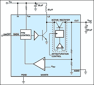
Figure 9. The internal synchronous rectifier in this boost regulator, the active rectifier, replaces the Schottky rectifier often used at that location.
An interesting side benefit of the pnp synchronous rectifier is its ability to provide both step-up and step-down action. For ordinary boost regulators, the input voltage range is limited by an input-to-output path through the inductor and the diode. (This unwanted path is inherent in the simple boost topology.) Thus, if VIN exceeds VOUT, the conduction path through the rectifier can drag the output upward, possibly damaging the load with overvoltage.
The pnp-rectifier circuit in Figure 9 operates in switch mode, even when VIN exceeds VOUT, with the active rectifier acting as the switch. This action is more akin to a regulating charge pump than to a buck regulator, because the buck mode of operation requires a second switch on the high side. The efficiency of Figure 9's circuit approximates that of a linear regulator: The efficiency is reasonably good over the voltage range of the four-cell battery (up to 6.2V).
Inverting-topology regulators that generate negative voltages, sometimes called buck-boost regulators, are useful applications for synchronous rectification. Like the boost topology, the inverting topology connects the synchronous rectifier in series with the output rather than to ground (Figure 10). In this example, the synchronous switch is an N-channel MOSFET with its source tied to the negative output and its drain tied to the switching node.
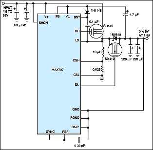
Figure 10. The inverting topology requires that the synchronous switch be in series with the output.
The circuit tricks the resulting 300kHz buck regulator into performing as an inverting-topology switcher by connecting the IC's GND pin to the negative output voltage instead of circuit ground. This switching regulator's efficiency of about 88% exceeds that of comparable asynchronous-rectifier supplies by 4%.
A similar version of this article appeared in the April 27, 1995 issue of EDN.
欢迎分享,转载请注明来源:内存溢出

 微信扫一扫
微信扫一扫
 支付宝扫一扫
评论列表(0条)