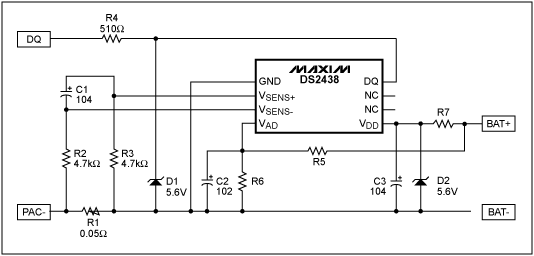
IntroductionDallas Semiconductor Battery Management ICs are designed to operate in cell packs for portable devices where the pack voltage at maximum would never exceed 10 volts. Adapting these devices for use in higher voltage cell packs is both simple and inexpensive. The example in this application note shows how to design a DS2438 into a high voltage circuit while maintaining proper ESD protection and accurate voltage and current measurements. Each component of the circuit shown in Figure 1 is described in detail below.

Figure 1. DS2438 circuit for handling cell voltages greater than 10 volts.
VDD RegulationZener diode D2 clamps the DS2438's supply preventing over voltage damage. The value of D2 must fall within the operating voltage range of the device, between 2.4 volt and 10.0 volt in this case. A value of 5.6 volt is recommended because it is close to the middle of the range. Because VDD is now clamped, voltage conversions off the VDD pin will no longer accurately reflect the true voltage of the cell pack. The VAD pin should be used for all voltage measurements.
Resistor R7 is used to prevent damage to the circuit by current limiting zener diode D2. The value chosen for R7 must be large enough to protect D2 when the cell voltage is at its maximum but small enough to allow the DS2438 to still operate when the cell voltage is at its minimum. The minimum resistance for R7 is dependent on the wattage rating of D2. The minimum value can be calculated from the following formula:

Where WD2 is the wattage rating of zener diode D2, VZD is the reverse bias rating of zener diode D2, and Vmax is the maximum possible voltage at node BAT+. Likewise, the maximum value for R7 can be calculated as:

Where Icircuit is the maximum current draw for the entire circuit, Vmin is the minimum possible voltage at node BAT+, and VZD is the reverse bias rating of zener diode D2. It is recommended that R7 be as large as possible to limit current load of the circuit and size and cost of diode D2.
VAD Pin MeasurementsResistors R5 and R6 form a voltage divider to limit the maximum voltage on the VAD pin to the maximum input level of the voltage A/D converter. The values of R5 and R6 should be large enough to prevent unnecessary drain on the cells, yet small enough that the parallel internal impedance of the VAD pin does not cause error in the measurement. A value of 10kΩ. for resistor R6 is recommended. The formula for calculating the value of resistor R5 is therefore:

Where Vmax is the maximum possible voltage at node BAT+ and Vvad is the maximum range of the voltage A to D input (10.0 volts for the DS2438). Cell pack voltage measurements should always be conducted from the VAD pin and the actual voltage can be calculated as:

For higher accuracy measurements, each unit can be individually calibrated with a precision voltage reference and the multiplier data stored inside the DS2438's user EEPROM.
ESD Protection and Noise SuppressionThe remaining components in the Figure 1 circuit are for ESD protection of the DS2438 and noise suppression on the A/D inputs. Their values are completely independent of the circuit supply voltage. Zener diode D1 and resistor R4 are recommended ESD protection for the DQ pin. Capacitors C1 and C2, and resistors R2 and R3 are for noise suppression on the sensitive voltage and current measurement pins. Capacitor C3 is a standard bypass capacitor on the IC's voltage input. Resistor R1 is the required external sense resistor for measuring current.
SummaryAdapting a Dallas Semiconductor Battery Management IC for use in higher voltage circuits requires minimal external components. The accuracy of the voltage measurements can be maintained either by using precision resistors or by individually calibrating each unit. All other device functions are unaffected by a higher supply voltage level.
欢迎分享,转载请注明来源:内存溢出

 微信扫一扫
微信扫一扫
 支付宝扫一扫
评论列表(0条)