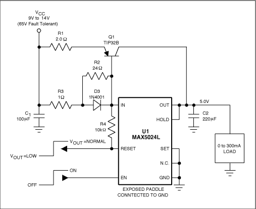
In Figure 1, the 5V linear regulator (U1) delivers as much as 150mA of load current when operaTIng by itself. OperaTIng with the external pass transistor shown (Q1), the circuit maintains 5V regulation while delivering more than 300mA.

Figure 1. An external pass transistor (Q1) more than doubles the output-current capability of this 5V linear regulator (U1).
The circuit accepts normal operating voltages in the range 9V to 14V, and delivers up to 300mA of load current at 5V. It withstands input transients to 65V, thanks to the IC's high input-voltage rating and internal thermal protection. A wide input-voltage range (6.5V to 65V) and temperature range of -40°C to +125°C make the circuit suitable for 12V and 48V automotive applications.
The external pass transistor increases the available load current by creating an additional path from input to output. The path in this case was designed for an additional 150mA, but you can obtain larger output currents by substituting other components in the circuit. To understand how the external transistor allows greater load currents, imagine the circuit with no output current. In that case the voltages at IN and the emitter of Q1 are approximately equal to VCC. Q1's base-emitter voltage is zero and the transistor is off.
As load current slowly increases from zero to 300mA, current begins to flow through U1 from VCC to OUT, causing a voltage drop across R3 and D3. The same voltage drop appears across R1 and the VBE of Q1. VBE increases as the load current increases. As VBE approaches the threshold of Q1, the transistor gradually turns on and allows current flow from the input to the load. Q1's VBE threshold is approximately 0.7V at room temperature, and decreases at higher temperatures to about 0.3V.
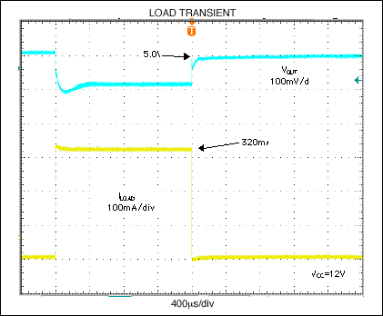
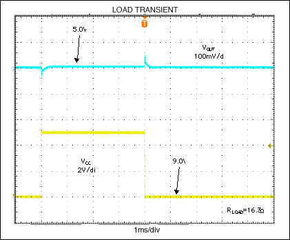
The transistor shown (TIP32B) is chosen for its power-dissipation capability and high collector-to-emitter voltage (-80V). The TO-220 package allows several watts of power dissipation, and the -80V collector-to-emitter voltage allows operation (with U1) in applications featuring input voltages as high as 65V. As illustrated by Figures 2-3, the circuit is stable in the presence of load and line transients.

Figure 2. Load transient (top trace) for the Figure 1 circuit.

Figure 3. Line transient (top trace) for the Figure 1 circuit.
This design idea appeared in the August 16, 2004 issue of EE Times magazine.
欢迎分享,转载请注明来源:内存溢出

 微信扫一扫
微信扫一扫
 支付宝扫一扫
评论列表(0条)