
Many applications require a controlled cycle during power-up and power-down. For older parts that operate on bipolar supply voltages (like DG401 switches), you should apply the most positive voltage first, a logic supply (possibly) next, and the negative supply voltage last. Violating this rule can cause "latch-up" within the semiconductor.
New families of ICs simplify the sequencing power to systems that require multiple supplies. We will describe these new ICs and their implementation after a discussion of discrete component approaches.
Simple RC ApproachA simple approach for sequencing the supply voltages of two or more circuits on the same rail is to simply introduce a delay between them by adding a series resistor and capacitor to ground on the power line. Only two discrete parts are required per line (Figure 1). However, this technique has many disadvantages: You should use it only for signal delays — not for power delays.
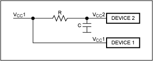
Figure 1. Power sequencing by an RC delay in the power line.
Delay depends on the rise time of the supply voltage. An RC approach isn't desirable for adding delay to a 3.3V supply voltage that's independent of the primary 5V supply, because 3.3V could come up first even with the delay. The 5V may not come up at all, which doesn't prevent 3.3V from being applied to the device. This approach might be acceptable if 3.3V is derived from 5V, but you must still consider the power loss in the resistor. As another consideration, the delayed supply voltage at power-down remains applied to the load longer than does the supply voltage that came up first.
A more reliable way to prevent one supply from coming up before another is to monitor the primary supply, to ensure it comes up first and reaches a certain level before the second supply turns on. Adding a small delay provides an additional reliability advantage. Figure 2 illustrates this approach for a system in which the power regulators are located in a remote power supply for example, and are therefore not accessible.
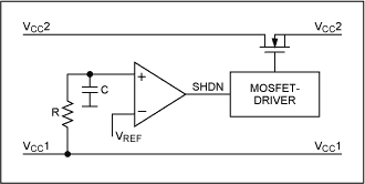
Figure 2. Power sequencing via RC , comparator, and MOSFET-driver.
The reference voltage on the negative input of the comparator sets the level to be reached by VCC - before VCC2 turns on. An RC combination on the other input adds a delay to the trigger. An n-Channel MOSFET switch guarantees no current flows in the VCC2 line, when power is off or when VCC1 has not yet reached the desired voltage. To fully enhance the MOSFET switch, a driver-generated gate-source voltage (VGS) exceeds VCC2 by several volts. The simplest driver can be a charge pump that doubles VCC2, which the comparator turns on and off via the charge pump's shutdown pin.
This approach also guarantees that VCC2 is shut down when VCC1 isn't present. Nevertheless, timing still depends on the rise time of VCC1, which may not be accessible to the designer. This arrangement allows a short interval-depending on the RC combination and the fall time of VCC1-in which VCC2 is present without VCC1. As another drawback, at least five components are needed to realize this function.
An attempt to implement the above circuit with a p-channel MOSFET (to eliminate the MOSFET driver) leads to the following problems. Full closure of a PMOS device cannot be guaranteed at power-up, because rise times of the gate and source voltages can be different, or must be controlled separately. The likely result is an output glitch at power-up, before the gate-source voltage (VGS) is small enough to close the MOSFET. At low voltages, additional resistance can appear in the power path because VGS isn't large enough to fully enhance the p-channel MOSFET.
The circuit above can easily be upgraded with standard reset ICs, and the result is fewer external components (Figure 3). Alternatives include the MAX809 (including voltage reference, comparator, fixed delay time, and reset threshold) and the MAX6301, for which the threshold and reset time are both adjustable. However, the main advantage is a more accurately adjustable timing that's also independent of the supply voltage rise and fall times. Moreover, VCC2 shuts down as soon as VCC1 falls below a certain threshold, so VCC2 is never present without VCC1.
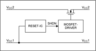
Figure 3. Sequencing with reset-IC, driver, and MOSFET. Power Regulator SequencingMany step-up and step-down regulators include a shutdown pin that can be used for power sequencing. First, you should examine whether the part in question fully shuts down, or whether input voltage is still present on the output (as is the case for many step-up regulators currently available). With suitable regulators, the desired sequencing can be accomplished with just an RC network on the shutdown input of one regulator (Figure 4). The RC delay ensures that VCC1 appears before VCC2. As for other RC circuits mentioned above, the VCC2 delay time also depends on the VCC1 rise timeҞso at power down, VCC2 may be present longer then VCC1.
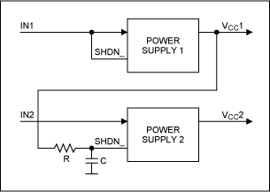
Figure 4. RC sequencing with power regulators.
For better reliability, a reset IC with integrated delay can control the power regulator's shutdown pin (Figure 5). Advantages include a defined timing behavior, a controlled power-down, and a guarantee that VCC2 shuts down before VCC1.
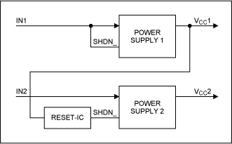
Figure 5. Reset sequencing with power regulators.
With a few external components, the MAX6819 or MAX6820 offer a simple way to control the power-up/power-down cycle of various power lines on a board. While monitoring a primary supply voltage, these devices enable/disable a secondary supply voltage via an external n-channel MOSFET switch (Figure 6). The circuit functions as described above, but with much less effort. The MOSFET driver, a regulated charge pump with VGS = 5.5V, is integrated along with the necessary capacitors in this SOT23 device.
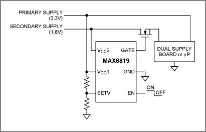
Figure 6. Power sequencing with the MAX6819.
The sequencers ensure that the MOSFET always has the minimum required VGS enhancement, which minimizes loss in the MOSFET and ensures a low drain-to-source impedance (RDS(ON)). The MAX6819 imposes a factory-set delay time of 200 ms, which occurs after the primary voltage rises above the set threshold and before enabling the charge pump to drive the external MOSFET switch.
The MAX6819 also has an Enable input that can override the internal circuitry and shut down or enable the external MOSFET. The MAX6820 allows users to simply adjust the delay time with a small external capacitor. Provided one supply is greater than 2.125V, either VCC1 or VCC2 can act as the primary source and thereby trigger the switch for the secondary supply.
Because some systems must sequence more than two supplies, the MAX6819 and MAX6820 support daisy chaining (Figure 7). All upstream power switches are disabled as long as power supplies upstream of the switches haven't reached their proper operation voltage, and the relevant delay time hasn't passed.
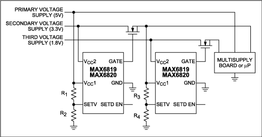
Figure 7. Sequencing three power supplies.
Sequencing Multiple SuppliesModern systems with more than two power supplies are now common. These power supplies usually have a power-up sequencing requirement. The MAX16029 quad-voltage monitor/sequencer circuit can provide a versatile and space-saving solution for this requirement (Figure 8). The MAX16029, packaged in a TQFN, can sequence up to four supply voltages with adjustable power-up delay.
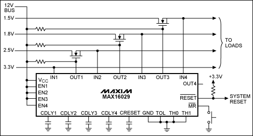
Figure 8. Sequencing four power supplies.
Reset SequencingIf you must control the reset timing rather than the power supply, you need a reset sequencer. This capability is necessary if, for example, a master CPU must be up and running before a slave CPU or a backplane ASIC. You can achieve the required sequencing by cascading two or more reset ICs like the MAX812, which include a manual reset input (MR). When the first supply voltage is up, and the first reset IC pulls its reset output high, the MR of the second IC is released and the internal timer starts running. After the delay time passes, the second reset is then deasserted.
The same function with some additional flexibility is provided in a single chip by the MAX6391/MAX6392 dual-voltage µP-supervisory circuits with sequenced outputs (Figure 9). These SOT23-8 parts monitor two supply voltages (master and slave), and provide two reset outputs with fixed or adjustable timeout periods.
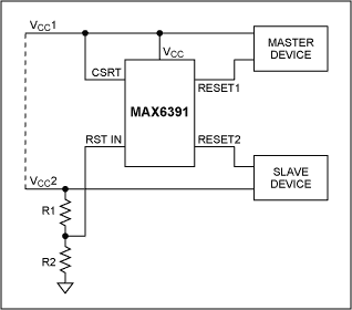
Figure 9. Reset sequencing with the MAX6391/MAX6392.
The chip asserts both resets when the master supply drops or hasn't reached its operating voltage. As long as the master reset is asserted, the slave reset can't be deasserted. At power-up and power-down, the sequenced reset outputs ensure that the slave part is never turned on when the master part isn't running. The voltage threshold and timeout period for the slave device are adjustable with a few external components.
A similar version of this article appeared in the April 2002 issue of Power Electronics magazine.
欢迎分享,转载请注明来源:内存溢出

 微信扫一扫
微信扫一扫
 支付宝扫一扫
评论列表(0条)