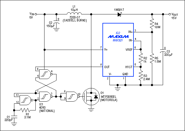

Figure 1. Consuming only microwatts of power, this 5V-to-15V boost converter provides low load currents with high efficiency.
IC2 compares its own reference voltage against the circuit output, VOUT. The resulTIng comparator output (pin 8) is high when VOUT is above its threshold and low otherwise. The quad NAND gate is configured as an oscillator, a set/reset latch, and a buffer inverter. The latch blocks oscillator pulses when the comparator output is high. When it goes low, the pulses pass through to Q1's gate and acTIvate the boost regulator.
R4 and R5 help determine the circuit's DC output level: VOUT = VREF(1 + R4/R5). The output voltage ripple for light loads depends on the comparator's hysteresis. With R3 = 2.4MΩ, the hysteresis in millivolts equals the value of R2 in kilohms. Then, the ripple in millivolts equals VREF(1 + R4/R5)(R2), where R2 is in kilohms. For this circuit, ripple = 1.182V(1 + 18/1.5)(1) = 15.4mV.

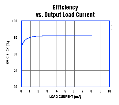
Figure 2. Efficiency in the Figure 1 circuit exceeds 90% for load currents between 1mA and 8mA.

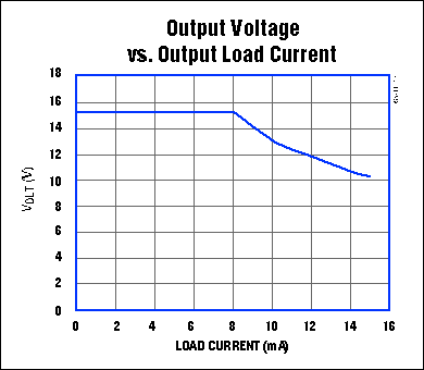
Figure 3. The oscillator frequency in Figure 1, set low to conserve power, also sets a sharp limit on load current.
欢迎分享,转载请注明来源:内存溢出

 微信扫一扫
微信扫一扫
 支付宝扫一扫
评论列表(0条)