
Table 1. Delay Vs. Programmed Value
Each half of the device can be programmed through separate input ports. Inputs A0 through A3 control side A output while inputs B0 through B3 control side B output. The inputs can either be held in a staTIc mode or changed dynamically. In the dynamic mode the data enable, setup and hold TImes must be met. Typically the delay to a valid output is 15 ns. During the transition period the outputs are in an undefined state. The pulse widths of the output will be a reproduction of the input delayed by the selected input delay value. Typical applications are included in the following section.
Each of the outputs is capable of driving 10 standard 74LS type loads. The device is compatible with both TTL and CMOS and is specified driving a 15 pF load. Input capacitance is 10 pF. All timing measurements are measured at 1.5 volts with the exception of rise and fall times. Input and output rise and fall times are measured between 0.6 volts and 2.4 volts.
Maximum Operational CharacteristicsThe DS1045 is capable of operation at a very high speed. Consideration should be given with respect to the minimum pulse width of the input signal when the maximum delay step is selected. For example, if a delay of a DS1045-5 of 84 ns is selected, then the input pulse width must not be shorter than 9 ns. Table 2 summarizes the minimum pulse widths (step zero delay), maximum delay times and the delay tolerance for each part number.
Table 2. Part Number Table
Block DiagramThe DS1045 is composed of a 16 stage delay line and two sets of digital multiplexers. Each side of the device can select an appropriate output delay stage by providing an input to the control code specified in Table 1. The binary value selects the individual stage of delay that becomes the output.
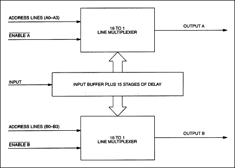
Figure 1. DS1045 Block diagram.
Circuit AnalysisIndividual stages may be thought of as RS flip-flops that have a variable capacitive load. Increasing the capacitive load increases the delay. Similarly, a decrease in the load capacitance decreases the delay. The operation of the variable capacitive load is similar to the operation of a varistor. The effect of this variable capacitive loading is that the individual stage set and reset times are precisely controlled. This process establishes controlled rise and fall times and improve the input to output waveform signal integrity of the device. The exact capacitive load is established at the factory in the final stages of the manufacturing process. A simplified schematic of the circuit is shown in Figure 2.
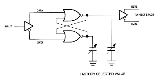
Figure 2. DS1045 Circuit diagram.
Family Step CharacteristicsFigure 3 indicates the general characteristic of each of the DS1045 devices in this family as a function of Binary Step Value Vs. Delay Time.
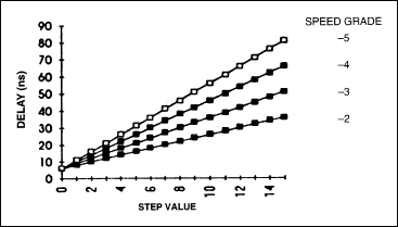
Figure 3. DS1045 Family delay by part type.
Step Linearity CharacteristicsFigure 4 indicates step linearity for rising and falling edge signals. Each of the devices exhibits a virtual straight line in step linearity. The device specification limits indicate that the starting delay of the zero position on the chart is the same for each of the devices (9ns).
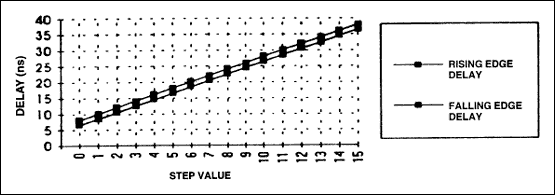
Figure 4. DS1045-2 Rising and falling edge delay times vs. step size.
This is due to the inherent delay of the first stage. The maximum deviation for any given step is indicated in Table 2. The maximum step tolerance is specified as ±2.5 ns for a DS1045-3 over the full binary range. The delay time at ste
Product DescriptionThe DS1045 is a 4-Bit Dual Programmable Delay Line that supports two programmable outputs from a single input. This CMOS device is capable of producing outputs in binary steps for maximum delays of up to 84 ns. The selection of one of four standard devices will allow steps of 2, 3, 4, or 5 ns. Table 1 indicates the standard product part for each delay and the maximum delay that can be obtained by each part.
Table 1. Delay Vs. Programmed Value
Each half of the device can be programmed through separate input ports. Inputs A0 through A3 control side A output while inputs B0 through B3 control side B output. The inputs can either be held in a static mode or changed dynamically. In the dynamic mode the data enable, setup and hold times must be met. Typically the delay to a valid output is 15 ns. During the transition period the outputs are in an undefined state. The pulse widths of the output will be a reproduction of the input delayed by the selected input delay value. Typical applications are included in the following section.
Each of the outputs is capable of driving 10 standard 74LS type loads. The device is compatible with both TTL and CMOS and is specified driving a 15 pF load. Input capacitance is 10 pF. All timing measurements are measured at 1.5 volts with the exception of rise and fall times. Input and output rise and fall times are measured between 0.6 volts and 2.4 volts.
Maximum Operational CharacteristicsThe DS1045 is capable of operation at a very high speed. Consideration should be given with respect to the minimum pulse width of the input signal when the maximum delay step is selected. For example, if a delay of a DS1045-5 of 84 ns is selected, then the input pulse width must not be shorter than 9 ns. Table 2 summarizes the minimum pulse widths (step zero delay), maximum delay times and the delay tolerance for each part number.
Table 2. Part Number Table
Block DiagramThe DS1045 is composed of a 16 stage delay line and two sets of digital multiplexers. Each side of the device can select an appropriate output delay stage by providing an input to the control code specified in Table 1. The binary value selects the individual stage of delay that becomes the output.

Figure 1. DS1045 Block diagram.
Circuit AnalysisIndividual stages may be thought of as RS flip-flops that have a variable capacitive load. Increasing the capacitive load increases the delay. Similarly, a decrease in the load capacitance decreases the delay. The operation of the variable capacitive load is similar to the operation of a varistor. The effect of this variable capacitive loading is that the individual stage set and reset times are precisely controlled. This process establishes controlled rise and fall times and improve the input to output waveform signal integrity of the device. The exact capacitive load is established at the factory in the final stages of the manufacturing process. A simplified schematic of the circuit is shown in Figure 2.

Figure 2. DS1045 Circuit diagram.
Family Step CharacteristicsFigure 3 indicates the general characteristic of each of the DS1045 devices in this family as a function of Binary Step Value Vs. Delay Time.

Figure 3. DS1045 Family delay by part type.
Step Linearity CharacteristicsFigure 4 indicates step linearity for rising and falling edge signals. Each of the devices exhibits a virtual straight line in step linearity. The device specification limits indicate that the starting delay of the zero position on the chart is the same for each of the devices (9ns).

Figure 4. DS1045-2 Rising and falling edge delay times vs. step size.
This is due to the inherent delay of the first stage. The maximum deviation for any given step is indicated in Table 2. The maximum step tolerance is specified as ±2.5 ns for a DS1045-3 over the full binary range. The delay time at step zero is the initial buffer delay of 9 ns ±1 ns.
Temperature CharacteristicsThe DS1045 exhibits excellent temperature characteristics. Figure 5 indicates how the change in delay times for each step is effected by temperature. The data was taken with a 5.0 volt supply voltage. A maximum total excursion (delta) of less than ±1 ns for both rising and falling edge signal are indicated.
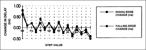
Figure 5. Temperature changes (0°C To 70°C).
Voltage CharacteristicsThe DS1045 is a voltage compensated device whose outputs, both rising and falling edges, vary less than 300 picoseconds with voltage excursions from 4.75 to 5.25 volts. Figure 6 indicates the values for each of the 16 delay steps.
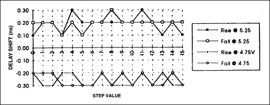
Figure 6. DS1045 Voltage compensation.
Delay Vs. Temperature: DS1045-3 Side A Rising Edge Signal @ Voltage = 4.75 Volts
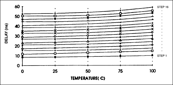
Side A Rising Edge Signal @ Voltage = 5.00 Volts
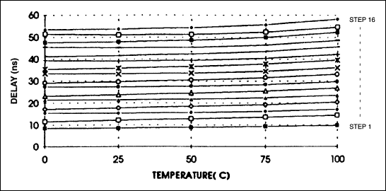
Side A Rising Edge Signal @ Voltage = 5.25 Volts
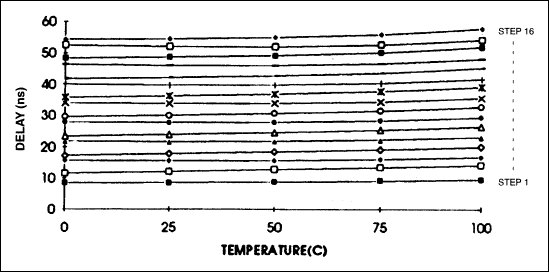
Side A Falling Edge Signal @ Voltage = 4.75 Volts
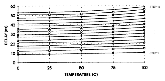
Side A Falling Edge Signal @ Voltage = 5.00 Volts
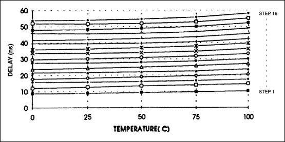
Side A Falling Edge Signal @ Voltage = 5.25 Volts
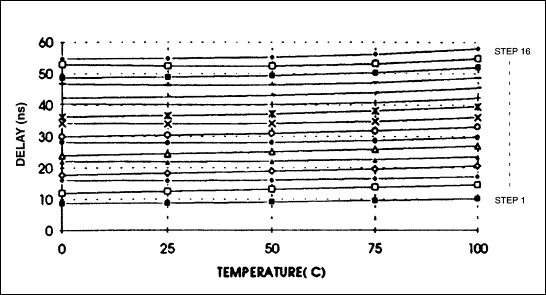
Delay Vs. Temperature: DS1045-4 (LOT#: 22804, DATE CODE: 4292A1)The following table indicates the performance of the DS1045-4 Programmable Delay. The plotted data is similar to the plots obtained for the DS1045-3. All steps are monotonic and show consistent variations with voltage and temperature.
VCC=4.75 Volts Rising Edge
VCC =5.0 Volts Rising Edge
VCC =5.25 Volts Rising Edge
VCC =4.75 VOLTS FALLING EDGE
VCC =5.00 Volts Falling Edge
VCC =5.25 Volts Falling Edge
DS1045-4 Delay Vs. Voltage CharacteristicsThe following chart indicates how the DS1045-4 delay changes for the positive and negative edges of step 1 and step 16 over voltage variations of 5 volts ±5%. For step 1, the falling edge starts at 7.923 ns and declines to 7.579 ns over an increasing voltage. The rising edge of step 1 follows a similar curve. For step 16, the slope is positive for increasing voltage. The exact values for each device are indicated in the following tables. Characteristics for the DS1045-3 and 5 are similar to the DS1045-4.
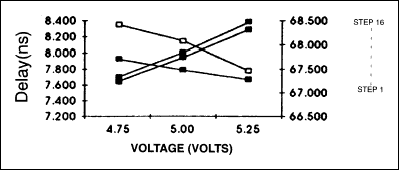
DS1045-4 Delay Vs. Voltage/Step
DS1045-3 Step Delay Variation Vs. Voltage
DS1045-4 Step Delay Variation Vs. Voltage
DS1045-5 Step Delay Variation Vs. Voltage
Operating Current Vs. Frequency
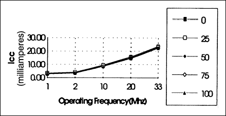
ICC Vs. Voltage and Temperature: DS10450-3 @ 4.75 Volts
DS1045-3 @ 4.75 Volts
DS1045-3 @ 5.00 Volts
DS1045-3 @ 5.25 Volts
Test ConsiderationsThe DS1045 is a high speed device and as such care should be exercised when testing. Good ground planes and power supply decoupling techniques should be used. It is also required that pin 2 be connected to VCC. A precision time interval counter is required with test resolution ten times better than the required data measurement.
Test ConditionsInput source: 50 ohms maximum with measurements taken at the 1.5 volt level.
Input signal pulse of 250 ns and a period of 1 ms.
Rise and Fall times of 3 ns between 0.6 and 3.0 volts.
Load Capacitance = 15 pF.
ApplicationsThe ability to use the DS1045 Dual Programmable Delay Line in multiple delay line applications makes it unique in the industry. It not only allows you to reduce inventory cost by having a lower number of parts in stock, but it also affords the designer the ability to improve system performance much later in the design cycle. All of the usual applications for delay lines are applicable to this part, but with much greater flexibility.
CautionA word of caution is in order when loading the input delay registers with the binary value of the desired delay function. In order to insure that the input signal integrity is maintained after the register has been loaded, the input signal must be allowed to propagate through the DS1045 for at least twice the selected delay value. For example, if you were using the DS1045-3, and selected a binary 8, then you should allow at least 32 ns times 2 or 64 ns before the input integrity is established.
欢迎分享,转载请注明来源:内存溢出

 微信扫一扫
微信扫一扫
 支付宝扫一扫
评论列表(0条)