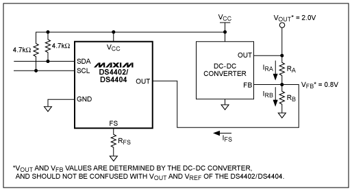
The Adjustable Power SupplyThe DS4402/DS4404 DACs contain two/four I²C adjustable current sources capable of sinking and sourcing current. A typical applicaTIon for these DACs is margining the output voltage of a DC-DC converter. (See Figure 1.)

Figure 1. DC-DC converter circuit with adjustable-current DACs used to margin the converter's output voltage.
The DS4402/DS4404 sink and source current from their OUT pins. Valid full-scale current values range from 0.5mA to 2.0mA. The value of the full-scale current, IFS, is determined by the size of the resistor connected to the DAC's FS pin of the corresponding OUT pin. The source/sink current generated by the DS4402/DS4404 is most commonly used to adjust the DC-DC converter's feedback voltage-divider.
Determining the RelaTIonship Between VOUT and IFSChoosing the right IFS depends on how much margin is desired on the DC-DC converter's VOUT pin. To determine this margin, we must discover the relaTIonship between VOUT and IFS.
Summing currents into the VFB node, we find that:

Where:

And:

However, since RB and VFB are constant, there is no change in IRB. Thus:

We are looking for the relationship between the margin on VOUT, ΔVOUT, and the selected range of IFS, ΔIFS. Since we know that the change in the IFS current equals the change in the current across RA, we subtract one set of VOUT and IRA values from another to determine the relationship between VOUT and IFS.
First, solving Equation 3 to find VOUT, we find that:

Use Equation 5 to create two equations. For one equation, we choose the maximum margin on VOUT, VOUTMAX, and the maximum IRA, IRAMAX. For the other equation, we choose the nominal values for VOUT and IRA, VOUTNOM and IRANOM. Subtracting the two equations, we get:

Using Equation 4, Equation 6 translates into the relationship:

Equation 7 shows that the relationship between the margin on VOUT and IFS is determined by the value of the resistor RA.
Calculating the Right Resistor Value for the Margin on VOUTNow that we know the relationship between VOUT and IFS, we can select the correct value of RA and, thus, RB to generate the desired margin on VOUT. Since the full-scale current sink/source range of the DS4402/DS4404 is 0.5mA to 2.0mA, we select 1mA as the IFS current for the DAC. To set this value, choose RFS based on the following equation (Equation 1 in the DS4402/DS4404 data sheet):

With VREF = 1.23V, we solve Equation 8 and find that RFS needs to be 9.53kΩ to produce a 1mA full-scale current.
With the DS4402/DS4404 IFS selected, we must determine the size of RA to achieve the desired margin on VOUT. A 2.0V VOUT with a 20% margin requires ±0.4V of change. Sinking and sourcing settings of the DS4402/DS4404 will manage the sign. The change in IFS equals the IFS value of 1mA, and the desired change in VOUT is 0.4V. After substituting for ΔVOUT and ΔIFS in Equation 7, we solve for RA and get RA = 400Ω.
Determining the Relationship Between RA and RBThe feedback network of the circuit in Figure 1 is a voltage-divider with resistors RA and RB. Looking at Figure 1 and assuming that IFS = 0A, we create a simple voltage-divider equation:

We assume that the desired nominal value for VOUT is 2.0V and that the DC-DC converter has a feedback voltage, VFB, of 0.8V. Substituting the values for VOUT and VFB, the relationship between RA and RB is determined:

We use Equation 10 to solve for RB, and get RB = 267Ω.
ConclusionThe resistive-feedback-divider network and the current-sinking/sourcing capabilities of the DS4402/DS4404 DACs control the margin of VOUT on a DC-DC converter. The relationship between the full-scale current, IFS, to the margin on VOUT is determined by the value of the resistor RA. By choosing the correct IFS value for your application, you can determine the correct resistor values for the feedback divider network, and achieve the desired margin on VOUT.
欢迎分享,转载请注明来源:内存溢出

 微信扫一扫
微信扫一扫
 支付宝扫一扫
评论列表(0条)