The MAX532 is a dual, 12-bit, voltage-output DAC. Access to the output amplifier's input terminals allows it to be easily configured as a programmable-gain amplifier (PGA) suitable for AC gain control.
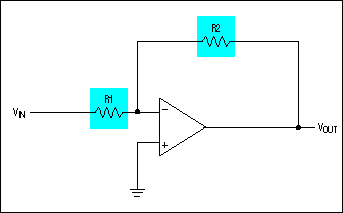
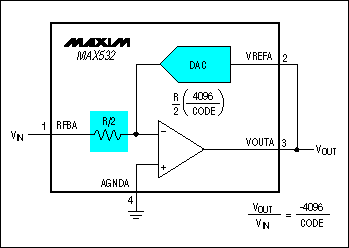
The circuit configuraTIon is that of an inverTIng amplifier, with R2 replaced by the effective resistance of the DAC ladder (Figure 1) and R1 replaced by internal feedback resistor RFB (Figure 2). In this circuit, an AC signal is applied to the feedback resistor input and the output signal is tied to the DAC reference input. The maximum signal at VOUT is limited by the amplifier's headroom from the supply rails (±12V to ±15V), which must be a minimum of 2.5V from either rail.

Figure 1. Fixed-gain inverting amplifier.

Figure 2. Programmable-gain amplifier.
The DAC functions as a programmable resistor in the feedback of the amplifier such that :
where R(DAC) is the resistance of the DAC ladder and RFB is the value of the feedback resistor, which is R/2.
R(DAC) = R/2×[4096/(DAC CODE)], with the DAC CODE given as a decimal value. As the code decreases, the effective DAC resistance increases, and so the gain increases. The transfer function for the circuit is thus:

The code can be programmed between 1 and full scale (212-1). Zero code is not allowed, as it results in the DAC's appearing as an open circuit in the feedback loop.
欢迎分享,转载请注明来源:内存溢出

 微信扫一扫
微信扫一扫
 支付宝扫一扫
评论列表(0条)