FPGA的IO支持多种电平标准,但是其中用几点的概念比较模糊,在此特意记下:
最近在用xilinx的spartan 6 与ARM进行通信,但是FPGA的逻辑电平是3.3V的LVTTL标准,而ARM输出的是1.8V的电平标准,两者IO电平的不匹配,出现了一些问题如下:
FPGA在VCCO = 3.3V是,是否可以设置FPGA的IO电平标准为1.8V?
在翻阅了《Spartan-6 FPGA SelecTIO Resources》后,得到了以下信息:Spartan-6的供电来源于3个引脚:VCCINT、VCCO、VCCAUX。
VCCINT is the main power supply for the internal FPGA logic. VCCINT also powers some of the available input drivers.
VCCINT主要为FPGA的内部逻辑单元供电,同时也会给一些输入供电。
The VCCO supplies, one for each of the I/O banks,power the output drivers and some of the input drivers. The voltage on the VCCO pins determines the voltage swing of the output signal.
Many of the low-voltage I/O standards supported by Spartan-6 devices require adifferent output drive voltage (VCCO). As a result, each device often supportsmulTIple output drive source voltages.
Output buffers within a given VCCO bank must share the same output drivesource voltage. The following I/Ostandards input buffers also use the VCCO voltage supply:
? LVCMOS25 (when VCCAUX = 3.3V)
? LVCMOS18_JEDEC
? LVCMOS15_JEDEC
? LVCMOS12_JEDEC
? PCI
? MOBILE_DDR
Spartan-6 FPGAs allow mulTIple I/Ostandards to be combined in the same device. Although the outputs are always powered byVCCO, mulTIple standards are available
under one of the five possible VCCO values. In addition, inputs often do notneed to match the voltage applied to VCCO. Further flexibility is achieved withmultiple VCCO levels in a single device.
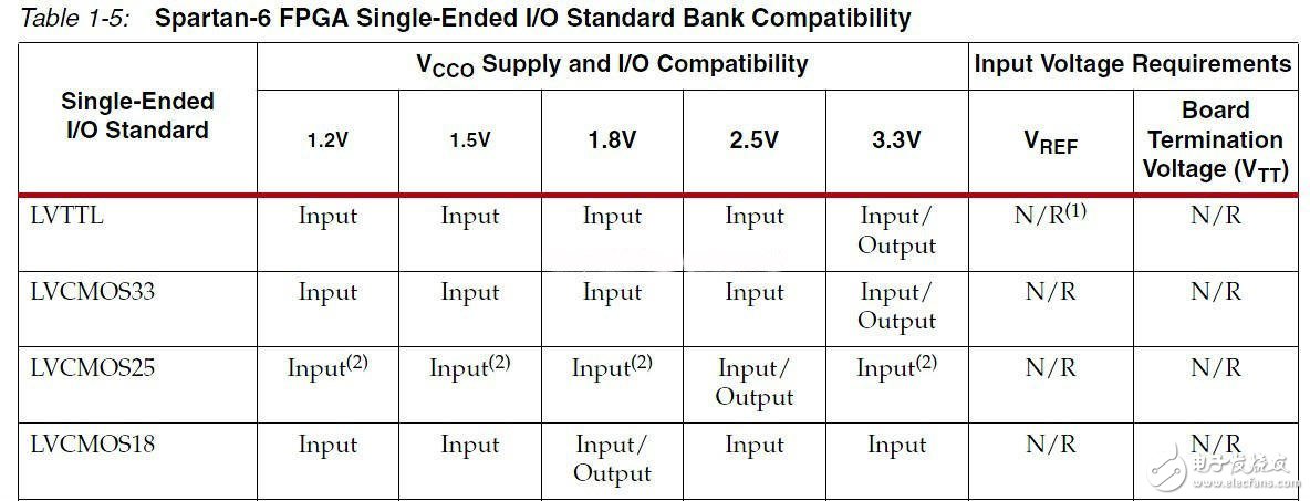
Each bank of I/Os has independent VCCO and VREF rails. This allows each bank to be powered at VCCO and VREF levels independent of how the other banksare set. VCCO provides power primarily to the I/O outputbuffers, and VREF supplies a reference voltage for HSTL and SSTL inputs. The VCCO pins are dedicated power pins and must bepowered at all times with a voltage rail from thePCB. However, the VREF pins are dual-purpose pins; they can be used as regular I/O pinsor VREF-supply pins. When a bank uses VREF-powered inputs (as an example, for the SSTL or HSTL standards), thedesign must use the VREF pins to supply the FPGA’s internal VREF rail with the reference voltage. If the SSTL or HSTL inputs are not used in a bank,the VREF pins in that bank can be used as regular I/O pins. Table 1-5 lists the VCCO and VREF requirements.

VCCO在FPGA中,每个Bank都有自己独立的VCCO,每个Bank的VCCO可以供不同的电源,以实现不同的Bank实现不同的IO标准,在同一个Bank中,VCCO只能是一个标准,通过上面的解释中,可以看到,IO的输出都是由VCCO供电的,也就是说每个Bank的IO输出电压决定于VCCO,同时部分标准的输入也是由VCCO提供电源的。在一个Bank中,输入的IO标准是可以不与VCCO相匹配的,如下图所示,VCCO为3.3V时,输入LVCMOS18的标准同样可以识别!
由此可见,对于3.3v的VCCO,输出的电平标准只能是3.3V,但是输入的标准可以是1.8V。
欢迎分享,转载请注明来源:内存溢出

 微信扫一扫
微信扫一扫
 支付宝扫一扫
评论列表(0条)