用于电信/数据通信的隔离式电源
Abstract: A 50W switching supply suitable for telecom applicaTIons is described. The supply, a high-frequency forward converter, provides an isolated 5V @ 10A with 1% line and load regulaTIon. A buck converter topology is selected after considering flyback and buck converters. The MAX5003 control IC is selected; its features and circuit are described. Important waveforms are shown and discussed; the power transformer is detailed; input, output, and feedback circuits are discussed. Performance is detailed and preferred PCB layout is provided.
Also see:
- MAX5003 QuickView Data Sheet
- MAX5003-50WEVKIT
- MAX5003EVKIT
- Design and simulate isolated power supplies with free MAX5003 Isolated Power Supply Design Software.
This 50W, isolated power-supply design can be used to replace purchased supplies with minimal addiTIonal engineering effort. The advantages of such an approach also include the accommodaTIon of custom footprint and substantially lower cost.
The ChallengePower supplies are often an afterthought. Purchased power-supply "bricks" are a quick solution, but with significant disadvantages, such as size, heat-sink and airflow requirements, long lead times, limited configurations, and higher overall costs. An in-house design usually fits product requirements better, but may not seem possible without a dedicated group of power-supply design engineers.
A few semiconductor companies are providing reference designs that can greatly streamline power-supply design and bring custom supply designs within reach. An "off-the-shelf design" makes it possible to quickly produce a supply that is smaller and simpler to integrate, performs better, and delivers much lower cost and superior time-to-market.
A kind of power supply that is currently in great demand is the telecom, datacom type. Such power supplies are utilized in central offices, PBXs, and servers, and typically use an input voltage of 36V to 72V. Their typical output power levels range from about 10W to 100W or even higher. Important requirements for these power supplies are galvanic isolation between primary and secondary, high efficiency over a wide input-voltage range, and ruggedness. The design of such power supplies, however, is relatively complex due to the requirements of isolation.
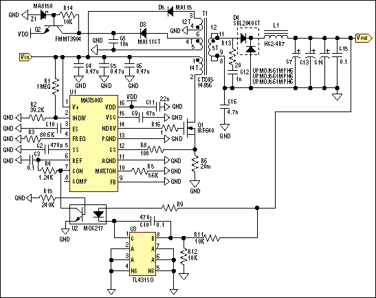
Figure 1 shows a 50W "off-the-shelf-designed" power supply. This is an isolated power supply with a 5V regulated output. Table 1 summarizes some of the target specifications.
Figure 1. Schematic diagram of ≈48V in and 5V out @ 10A isolated power supply.
Table 1. Summary of Target Specifications
Power Circuit Topology
Among the several power topologies available, the single transistor forward topology offered the simplest lower-cost solution while providing very good efficiencies throughout the operating power range. This topology, however, requires a transformer reset winding that is connected to pins T1-3 and T1-4. The forward converter was chosen, because it offers higher power density and higher efficiency than a flyback converter at these power levels. Although first-order flyback topology schematics tend to look simpler, these converters are more difficult to deal with (see the brief comparison below). Transformer T1 provides the necessary isolation between primary and secondary, in this case 1500V. In addition, efficiency is improved by powering the control circuit in the primary (T1-5, T1-6 leads) after initial startup. A 250kHz switching frequency was selected to allow for minimization of the energy storage components, such as transformers.
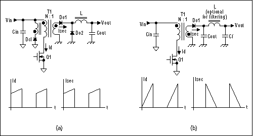
Figure 2a shows the power-stage configuration of a forward converter. Power transfer to the secondary-side circuit takes place when the power switch Q1 is turned on. Almost all forward supplies are operated in continuous conduction mode, which means that the inductor energy is not completely depleted before the start of the next cycle. The drain current Id looks rectangular with a slight pedestal. When Q1 turns off, Do1 reverse-biases, whereas Do2 forward-biases, carrying the entire inductor current. The reset winding that is connected to the cathode of Dcl allows for the recycling of the energy stored in the transformer core by returning it to the input source.
Figure 2b shows the power stage of a flyback converter. In this case, power transfer to the secondary takes place after Q1 has turned off. Energy stored in the transformer core is delivered to the load. Flyback converters tend to cost less for lower-power applications, because they don't require an output inductor. A small filtering inductor is sometimes used, however, to reduce high-frequency spikes that are present at the output voltage. Flyback converters are often operated in discontinuous mode, which means that the energy stored in the transformer is transferred completely to the output before the start of the next cycle.
Figure 2. Forward (a) and flyback (b) power topologies.
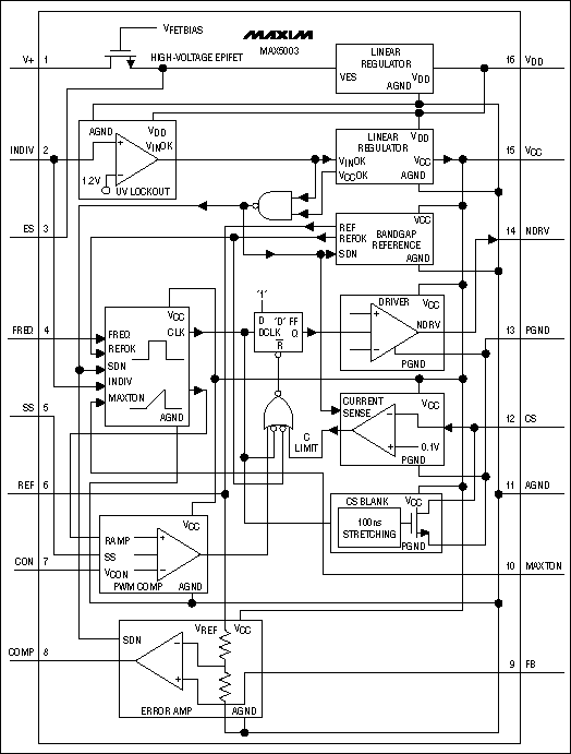
The primary-side control circuit is based on the MAX5003. A simplified block diagram of this IC is shown in Figure 3. The MAX5003 represents the next generation of power-supply controllers that integrate many functions that are necessary for the design of telecom power supplies. It contains a high-voltage startup circuit that speeds up the initial power-up process. It also has other abilities that ease the design of isolated, regulated, telecom power supplies, such as voltage feed-forward compensation. Voltage feed-forward is an important element of the design, because it helps to provide constant power-stage gain that results in more stable voltage control loops. It also significantly helps with input supply rejection by instantly responding to varying input voltages and correcting the duty cycle within a single cycle without the intervention of the slower-voltage control loop.
Figure 3. MAX5003 block diagram.
The following equations should help you understand the effect of feed-forward compensation. The large signal modulator and power-stage gains of a forward converter without feed-forward compensation are given in equations (1) and (2), respectively.
 (1)
(1)
欢迎分享,转载请注明来源:内存溢出
 微信扫一扫
微信扫一扫
 支付宝扫一扫

评论列表(0条)