80mA Precision Reference,80ma精密基准电压源
Abstract: This applicaTIon note presents a circuit that adds a transistor buffer in the error-amplifier feedback loop of a voltage-reference IC. This configuraTIon boosts the output-current capability to 80mA without degrading the IC's output accuracy. The MAX6033A voltage reference is featured in the design.
This design idea appeared in the July 10, 2006 issue of Portable Design magazine.
Large analog systems that impose many loads on the reference voltage often demand more current than a single voltage-reference IC can deliver. A common soluTIon is to add a buffer circuit at the reference-IC output, but reference accuracy is then degraded by the buffer's offset voltage. This arTIcle presents an alternative approach to the problem.
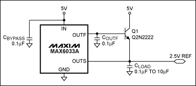
A better solution is to put the buffer inside the feedback loop of the reference error amplifier. The buffer then has no effect on reference accuracy. That configuration is, however, possible only for reference ICs in which the loop is accessible to users. The MAX6033A voltage reference in Figure 1 provides output force and sense pins for that purpose. The device also features a SOT23 package, 0.04% initial accuracy, and a 7ppm/°C temperature coefficient.
Figure 1. Adding a transistor buffer in the error-amplifier feedback loop of this voltage-reference IC boosts the output-current capability (to 80mA, in this case) without degrading the IC's output accuracy.
The smallest and most economical buffer is a simple NPN transistor in the IC's error-amplifier loop, as shown here. The 2N2222 has been a favorite for decades. The transistor has no effect on the reference output accuracy, provided that its base-current demand does not exceed drive limits on the OUTF pin. That pin can drive 10mA to within 200mV (nominal) of the voltage at IN, and to within 500mV over the temperature range -40°C to +125°C. The circuit shown generates a 2.5V reference from a 5V supply, so the transistor's worst-case VBE (1.2V) requires a 3.7V drive from the OUTF pin—this is well below the 500mV worst-case headroom limit. Note that worst-case VBE values prevent the use of this technique for a 4.096V reference on a 5V supply, or a 2.5V reference on a 3.3V supply.
The transistor's power-dissipation limit imposes a maximum output current for this circuit, and is chosen to be 80mA. The transistor can dissipate 350mW at +25°C, and is derated at 2.8mW/°C. At +70°C, the limit is, therefore, 224mW. The transistor drops 2.5V, so the maximum allowable current is 89mA. For a worst-case beta of 35, the transistor requires a worst-case base current of only 2.3mA, which is well within the OUTF pin's current-drive capability. With appropriate transistors, you can increase this output current to any reasonable level.
The MAX6033A requires 0.1µF ceramic capacitors on the IN and OUTF pins for stability. The OUTF capacitor determines the circuit's response speed, but the transistor buffer does not have a significant effect on the circuit's transient response. DC references seldom have enough transient response to manage fast step loads, so you must rely on the output capacitor to supply any fast current spikes. For this buffer circuit, the capacitor on the transistor emitter supplies current for fast load steps. The circuit has been tested with capacitive output loads up to 10µF.
欢迎分享,转载请注明来源:内存溢出

 微信扫一扫
微信扫一扫
 支付宝扫一扫
评论列表(0条)