NonvolaTIle STANDBY/ON Switch
Abstract: Using an electronically programmable voltage reference (DS4305) as a single-bit nonvolaTIle memory cell, this circuit remembers the state of a STANDBY/ON switch that changes state with no operator present.
This design idea appeared in the September 3, 2009 issue of EDN magazine.
The following STANDBY/ON switch is suitable for applicaTIons (industrial and telecom, for instance) in which the circuitry must somehow "remember" its state (STANDBY or ON) after a power failure that occurs when no operator is present. An alternaTIve approach based on a battery (or supercapacitor) and flip-flop is less reliable, because its state can be lost if leakage current drains the battery. Another alternative involves the use of a microcontroller and EEPROM, but that requires software plus a provision for startup time. Also, a stand-alone EEPROM for this application has an awkward interface.
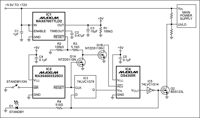
The idea (Figure 1) is to use an electronically programmable voltage reference (IC4, DS4305) as a single-bit nonvolatile memory cell. To remember the state of the STANDBY/ON switch, this circuit programs the output voltage high or low, and can reprogram it a minimum of 50,000 times.
Figure 1. If power fails with no operator present, this circuit remembers its state (STANDBY or ON).
IC1 (MAX6766) is a low-dropout (LDO) linear regulator with RESET output, and a wide input-voltage range that extends up to 72V. A µP supervisor (IC2, MAX6468) debounces the control button (the STANDBY/ON pushbutton), and supports the programming of IC4 by increasing the pause length between pulses. The IC4 output drives an inverter with Schmitt-trigger input (IC5), which in turn drives the gate of transistor Q2 to control the main power supply.
Flip-flop IC3 helps to change the STANDBY/ON state with each press of the control button. At the end of the IC4 programming cycle, a low-to-high edge at IC3's CLK input sets the flip-flop to its opposite state, thanks to the feedback from the inverter. This action is also triggered by IC2 RESET at power-up, to ensure that the switch is ready to change state. Transistor Q1B and the RESET output of IC1 prevent the programming of incorrect states by blocking IC4's ADJ input during startup and power-fail conditions.
The effect of IC2's power-up (or -down) RESET pulse on IC4's ADJ input must also be blocked; IC1's RESET timeout is therefore set (by capacitor C2) to be longer than the RESET timeout of IC2. The voltage threshold of IC2 (2.9V) is also lower than that of IC1 (4.6V). The worst-case "low" input threshold for IC5 (1.32V) guarantees the STANDBY position at first power-on, because the factory-preset output for IC4 is only 1.2V.
欢迎分享,转载请注明来源:内存溢出

 微信扫一扫
微信扫一扫
 支付宝扫一扫
评论列表(0条)