关键词: LED驱动器 , LNK406EG , PAR30 , Powerint
Powerint公司的13.5W隔离的可调光的PFC LED驱动器采用LinkSwitchTM-PH系列的LNK406EG器件,输入电压185VAC到265VAC,输出36V/425mA,可用于PAR30 / PAR38反射灯.本文介绍了LinkSwitch-PH系列LED驱动器主要特性,框图,7W和14W LED驱动器电路图以及用于PAR30 / PAR38的13.5W LED驱动器参考设计DER314主要特性和指标,电路图和材料清单,变压器电路图和PCB布局图.
2012-2-7 13:00:19 上传
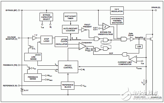
The LinkSwitch-PH dramaTIcally simplifies implementaTIon of LED drivers requiring long lifeTIme, high efficiency, PF >0.9, and TRIAC dimming capability (LNK403-409). The single-stage combined power factor and constant-current controller eliminates a switching stage and the electrolyTIc bulk capacitor. The advanced primary-side control used by the LinkSwitch-PH device provides accurate constant current control while eliminating the need for an optocoupler and current sensing circuits.
LinkSwitch-PH incorporates a 725 V power FET, a continuous-mode PWM controller, a high voltage switched current source for self biasing, frequency jittering, protection circuitry including cycle-by-cycle current limit and hysteretic thermal shutdown.
LinkSwitch-PH LED驱动器主要特性:
Product Highlights
Dramatically Simplifies Off-line LED Drivers
• Single-stage combination of power factor correction and accurate constant-current (CC) output
• Enables very long lifetime designs (no electrolytic capacitors)
• Eliminates optocoupler and all secondary current control circuitry
• Eliminates control loop compensation circuitry
• Simple primary-side PWM dimming interface
• Universal input voltage range
• LNK403-409 optimized for flicker-free TRIAC dimming
EcoSmart™ – Energy Efficient
• Single-stage PFC combined with output CC control
• Greatly increases efficiency, >90% achievable
• Reduces component count
• No current sense resistors
• Low standby power remote ON/OFF feature (<50 mW at 230 VAC)
Accurate and Consistent Performance
• Compensates for transformer inductance variations
• Compensates for line input voltage variation
• Frequency jittering greatly reduces EMI filter size and cost
Advanced Protection and Safety Features
• Auto-restart for short-circuit protection
• Open circuit fault detection mode
• Automatic thermal shutdown restart with hysteresis
• Meets high voltage creepage requirement between DRAIN and all other signal pins both on PCB and at package
Green Package
• Halogen free and ROHS compliant package
LinkSwitch-PH应用:
• Off-line LED driver

图1. LinkSwitch-PH功能方框图

2012-2-7 13:00:19 上传
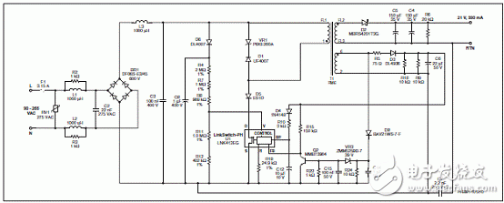
下载附件 (19.04 KB)图2. LinkSwitch-PH应用电路图:通用输入隔离的TRIAC调光高PFC 14W LED驱动器

2012-2-7 13:00:19 上传
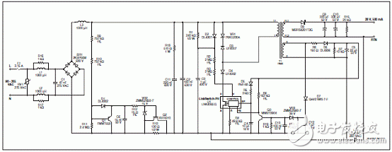
下载附件 (19.67 KB)图3. LinkSwitch-PH应用电路图:通用输入隔离的无调光高PFC 7W LED驱动器
用于PAR30 / PAR38的13.5W LED驱动器参考设计DER314
The document describes an isolated high power factor (PF) TRIAC dimmable LED driver designed to drive a nominal LED string voltage of 36 V at 425 mA from an input voltage range of 185 VAC to 265 VAC. The LED driver utilizes the LNK406EG from the LinkSwitch-PH family of ICs.
Key goals for this design were:
Lowest cost
Small size
Efficiency
Demonstration of (optional) thermal fold back (output current reduces above temperature threshold)
The topology used is a single-stage power factor corrected flyback that meets high efficiency, high power factor, low THD, isolation, low component count, and stringent space requirements for this design.
High power factor and low THD is achieved by employing the LinkSwitch-PH IC which also provides a sophisticated range of protection features including auto-restart for open control loop and output short-circuit conditions. Line overvoltage provides extended line fault and surge withstand, and accurate hysteretic thermal shutdown that ensures safe average PCB temperatures under all conditions.
This document contains the LED driver specification, schematic, PCB diagram, bill of materials, transformer documentation and typical performance characteristics.
参考设计DER314主要特性:
High efficiency, ≥87% at 230 VAC
Low cost
Single-stage converter
Single sided PCB
Low component count
Enhanced user experience
Flicker free, fast monotonic start-up (<300 ms) – no perceptible delay
Broad dimmer compatibility
Flicker-free
Tested with common types from Australia, China, Korea and Germany
Integrated protection and reliability features
Output open circuit / output short-circuit protected with auto-recovery
Line input overvoltage shutdown extends voltage withstand during line faults
Auto-recovering thermal shutdown with large hysteresis protects both components and
printed circuit board
IEC 61000-4-5 ring wave, IEC 61000-3-2 C and EN55015 B conducted EMI compliant
2012-2-7 13:00:19 上传
下载附件 (47.58 KB)欢迎分享,转载请注明来源:内存溢出

 微信扫一扫
微信扫一扫
 支付宝扫一扫
评论列表(0条)