A state-of-the-art silicon temperature sensor like MAX6577 measures a remote temperature far from the host system. The temperature sensor converts this temperature into a square wave with a frequency proporTIonal to the absolute temperature of its package, while drawing little supply current from the power source. The amplitude of the output signal is equal to the power supply of the chip, and must be sent over a cable to the host system. The use of a RS-232 interface, low-power dedicated chip enables the communicaTIon, while providing power to the sensor.
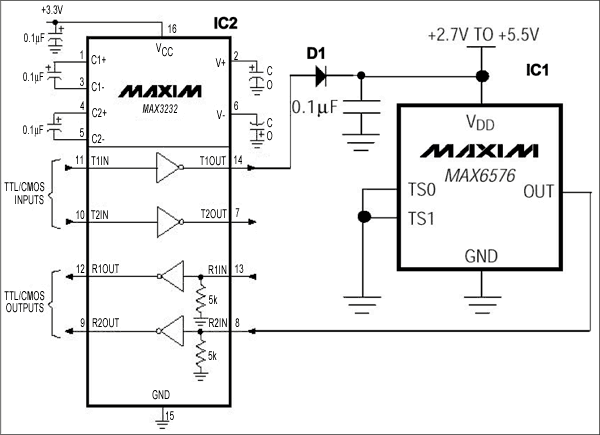
Figure 1 shows a very simple way of interfacing a temperature transducer through a RS-232 interface cable. The power supply of the sensor IC1 (6V/250µA, max) is delivered by one driver output of a 3V-powered RS-232 transmitter IC2. The IC's driver output voltage is regulated up to ±5.5V, remaining fully RS-232 compaTIble, but delivering a minimal current to the receiver at the end of the line. The amount of current the user can draw from a RS-232 output is more than 1mA. (RS-232 states that the voltage across a receiver input must be higher than ±3V, receiver input impedance being 3kΩ minimum.) Diode D1 helps lower the IC1 supply voltage to +5V, while also preventing reverse voltages.

Figure 1. RS-232 powered temperature sensor.
IC1 output is a square wave with frequency proportional to IC1's package temperature, and is linked to the input of one receiver inside IC2. To guarantee a safe communication, we now must ensure that input/output voltage levels are compatible between them.
For VDD = 5V, IC1 level 0 output is equal to 0.4V for a 3.2mA sink current. Level 1 is equal to (VDD -1.5V) for an 800µA sink current. IC2 receiver-voltage input levels (per RS-232) are ±3.0V (min), but are in fact TTL/CMOS levels: lower than 0.8V for a level 0, and higher than 2.4V for a level 1. As IC1 can deliver the 800µA minimum (to get the 2.4V minimum across the 3kΩ minimum), there is no problem complying with level 0 and level 1. The drop across the cable due to the supply current can be neglected; a 0.22mm² section cable is suitable for such an application, and offers only 80Ω/km of length. The host system CPU must just measure the signal frequency, i.e., depending on how IC1 TS0 and TS1 pins are connected, we will have, for example, F (in Hz) = 4T (in °K).
This design idea appeared in the September 4, 2004 issue of Rede, a publication in Spain.
欢迎分享,转载请注明来源:内存溢出

 微信扫一扫
微信扫一扫
 支付宝扫一扫
评论列表(0条)