
Freescale公司的三相BLDC/PMSM低压马达控制方案采用MC9S08AC16系列器件.这种8位MCU采用增强的HCS08内核,具有低成本和高性能,系列有各种模块,存储器容量,存储器类型和封装形式.MC9S08AC16和MC9S08AC8用于消费类电子和工业,MC9S08AW16A和MC9S08AW8A用于汽车电子.本文介绍了MC9S08AC16系列主要特性,方框图,以及三相BLDC和PMSM低压马达控制方案主要特性,详细电路图以及材料清单(BOM).
3-Phase BLDC/PMSM Low- Voltage Motor Control Drive
The MC9S08AC16 Series devices are members of the low-cost, high-performance HCS08 Family of 8-bit microcontroller units (MCUs). All MCUs in the family use the enhanced HCS08 core and are available with a variety of modules, memory sizes, memory types, and package types.
MC9S08AC16 Series Devices
• Consumer & Industrial
— MC9S08AC16
MC9S08AC8
• AutomoTIve
— MC9S08AW16A
— MC9S08AW8A
8-Bit HCS08 Central Processor Unit (CPU)
• 40-MHz HCS08 CPU (central processor unit)
• 20-MHz internal bus frequency
• HC08 instrucTIon set with added BGND instrucTIon
• Background debugging system
• Breakpoint capability to allow single breakpoint setTIng during in-circuit debugging (plus two more breakpoints in on-chip debug module)
• Debug module containing two comparators and nine trigger modes. Eight deep FIFO for storing change-of-flow addresses and event-only data. Debug module supports both tag and force breakpoints.
• Support for up to 32 interrupt/reset sources
Memory Options
• Up to 16 KB of on-chip in-circuit programmable FLASH memory with block protection and security options
• Up to 1 KB of on-chip RAM
Clock Source Options
• Clock source options include crystal, resonator, external clock, or internally generated clock with precision NVM trimming
System Protection
• Optional computer operating properly (COP) reset with option to run from independent internal clock source or bus clock
• Low-voltage detection with reset or interrupt
• Illegal opcode detection with reset
• Illegal address detection with reset
Power-Saving Modes
• Wait plus two stops
Peripherals
• ADC — 8-channel, 10-bit analog-to-digital converter with automatic compare function
• SCI — Two serial communications interface modules with optional 13-bit break
• SPI — Serial peripheral interface module
• IIC — Inter-integrated circuit bus module to operate at up to 100 kbps with maximum bus loading; capable of higher baud rates with reduced loading
• Timers — Three 16-bit timer/pulse-width modulator (TPM) modules — Two 2-channel and one 4-channel; each has selectable input capture, output compare, and edge-aligned PWM capability on each channel. Each timer module may be configured for buffered,centered PWM (CPWM) on all channels
• KBI — 7-pin keyboard interrupt module
Input/Output
• Software selectable pullups on ports when used as inputs
• Software selectable slew rate control on ports when used as outputs
• Software selectable drive strength on ports when used as outputs
• Master reset pin and power-on reset (POR)
• Internal pullup on RESET, IRQ, and BKGD/MS pins to reduce customer system cost
Package Options
• 48-pin quad flat no-lead package (QFN)
• 44-pin low-profile quad flat package (LQFP)
• 42-pin shrink dual-in-line package (SDIP)
• 32-pin low-profile quad flat package (LQFP)
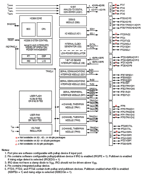
图1.MC9S08AC16系列方框图
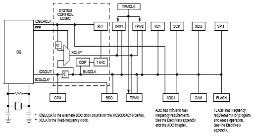
图2.MC9S08AC16系统时钟分布方框图
三相BLDC/PMSM低压马达控制驱动方案
Freescale’s 3-Phase BLDC/PMSM Low-Voltage Motor Control Drive is a 3-phase power stage that will operate with DC input voltages in the range 12–24 V, 4 A. Together with the daughter boards, it provides a software-development platform that allows algorithms to be written and tested without designing and building any hardware. It supports a variety of algorithms for PMSM and brushless DC (BLDC) motors.
The 3-Phase BLDC/PMSM Low-Voltage Motor Control Drive contains reverse-polarity protection circuitry, MOSFET-gate-drive circuits, analog-signal conditioning, low-voltage power supplies and bridge MOSFETs. The power devices do not need to be mounted on a heatsink.
There are controller daughter boards available with these controllers:
•MC56F8013/23 — LQFP32
•MC9S08AC16 — LQFP44
•MCF51AC256 — LQFP80
•MC9S08MP16 — LQFP48
•MC56F8006 — LQFP32
板主要特性:
•Power supply voltage input 12–24 V DC, extended up to 50 V (see chapter 2.2 Electrical Characteristics for details)
•Output current 4 A
•Power supply reverse polarity protection circuitry
•3-phase bridge inverter (6 MOSFET’s)
•3-phase MOSFET gate driver with overcurrent and undervoltage protection
•3-phase and DC-bus-current-sensing shunts
•DC-bus voltage sensing
•3-phase back-EMF voltage-sensing circuitry
•Low-voltage on-board power supplies
•Encoder/hall sensor sensing circuitry
•Motor power and signal connectors
•2 connectors for daughter board connection
•CAN physical layer
•USB interface
•User LED, power-on LED, 6 PWM LED diodes, and SCI activity LED diodes
•Up, down, toggle switches
•Reset push-button
图3.三相BLDC/PMSM低压马达控制驱动板外形图
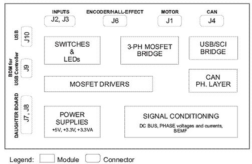
图4. 控制驱动板方框图
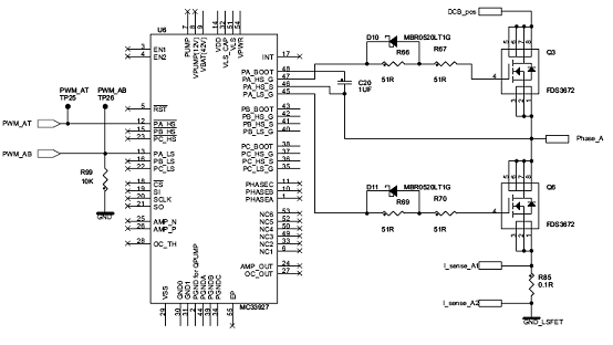
图5. 相位输出电路图
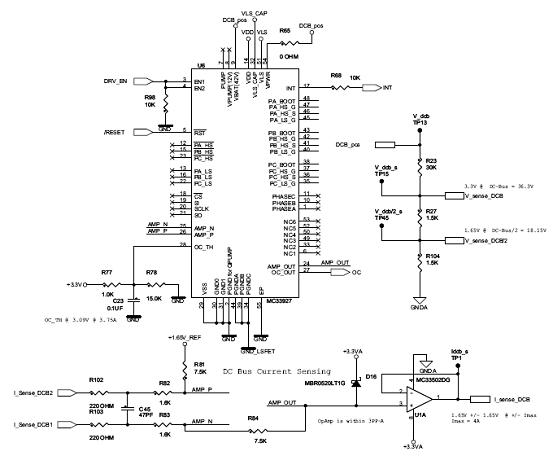
图6. 总线反馈电路图
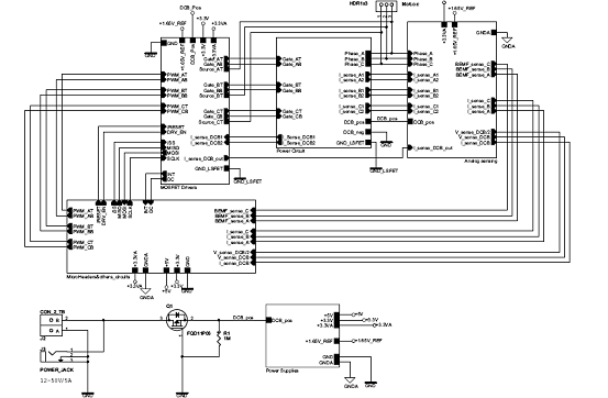
图7. 控制驱动板电路图
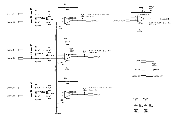
图8. 控制驱动板电路图:模拟检测-相电流检测
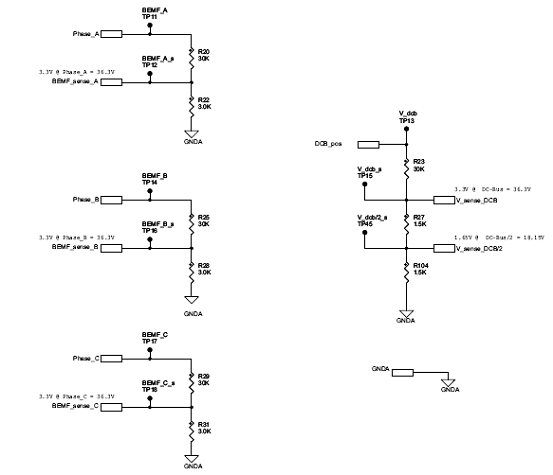
图9. 控制驱动板电路图:模拟检测-后EMF检测
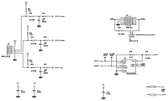
图10. 控制驱动板电路图:微插头和其它电路-编码器/霍尔传感器和CAN
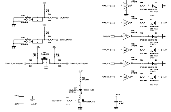
图11. 控制驱动板电路图:微插头和其它电路-开关,用户和PWM LED
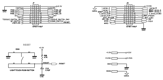
图12. 控制驱动板电路图:微插头和其它电路-子板连接器和RESET
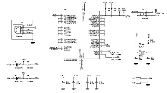
图13. 控制驱动板电路图:微插头和其它电路-USB/SCI桥
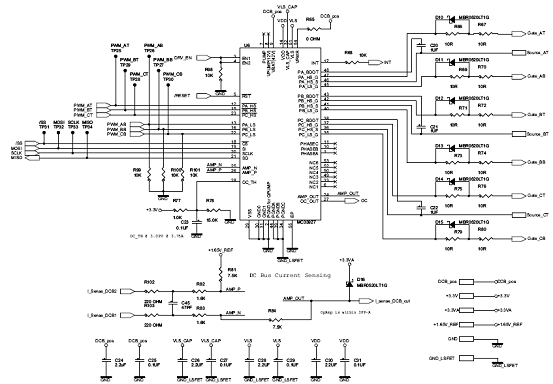
图14. 控制驱动板电路图:MOSFET驱动器
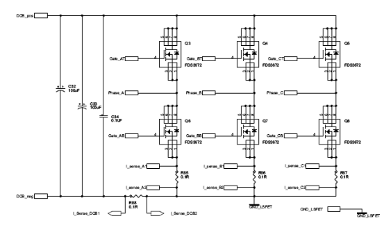
图15. 控制驱动板电路图:电源电路
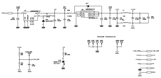
图16. 控制驱动板电路图:电源电路(2)
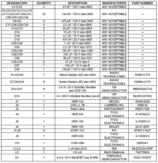
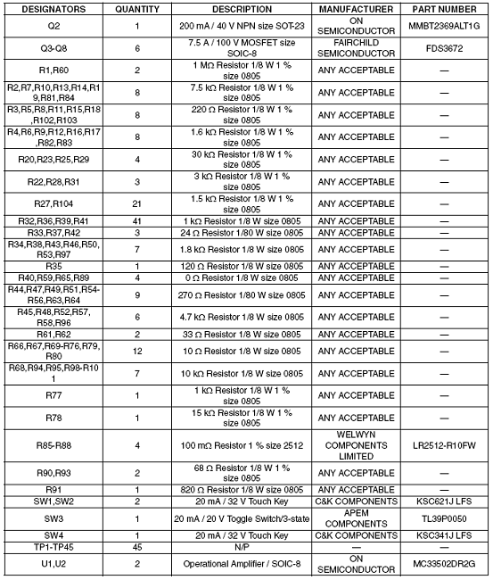
控制驱动板材料清单(BOM):

推荐课程:
张飞软硬开源,基于STM32 BLDC直流无刷电机驱动器视频套件
https://t.elecfans.com/topic/42.html?elecfans_trackid=fsy_post
欢迎分享,转载请注明来源:内存溢出

 微信扫一扫
微信扫一扫
 支付宝扫一扫
评论列表(0条)