As explained in the discussion that follows, a designer with adequate knowledge of the linear and switching regulators currently available can readily achieve efficient operaTIon in 5V/3.3V systems. Such systems include portable computers, which generally require step-down conversion, and personal digital assistants (PDAs), which generally require step-up conversion. Minimal current consumption is possible in both cases.
You can always generate the necessary supply voltages with multiple regulators, whether step-up or step-down conversion is required. As an alternative, you can choose a single IC that delivers both. Other topics to be covered here are the next generation of single-IC, dual 3.3V/5V step-down regulators, and ICs that generate highly accurate supply voltages for high-speed processors such as the Pentium, Pentium Pro, and Power PC. Two-Regulator Step-Down ConfigurationsThree practical topologies are available for deriving 5V and 3.3V (for instance) from a single input voltage using two step-down regulators. They are separate 5V and 3.3V switching regulators connected in parallel to the input voltage, a 5V switcher connected to the input and powering a 3.3V switcher, and a 5V switcher connected to the input and powering a 3.3V linear regulator. A fourth possibility—two linear regulators in series or parallel—is too inefficient for most applications.
The most efficient approach comprises two switching regulators connected to the input. The second approach—a 3.3V switcher powered by a 5V switcher—looks attractive at first, because the second switcher drops less voltage (5V minus 3.3V) and therefore dissipates less power. Nevertheless, the overall efficiency for 3.3V conversion (5V-converter efficiency times that of the 3.3V converter) is fairly poor. Either way, the use of two switching converters gives you the highest efficiency. It also gives you the highest cost and the most noise, and takes the most PC-board area.
The third topology is promising if the linear regulator delivers only a moderate amount of current. If this regulator's internal supply current is much less than its output current, then its efficiency is simply VOUT/VIN times 100. Thus, a linear regulator converts 5V to 3.3V with an efficiency of 66%. That amount of power loss can be acceptable for some applications, but remember that 66% must be multiplied by the 5V-switcher efficiency to obtain the overall efficiency for 3.3V conversion.
Power-supply efficiency measures the amount of power wasted in the supply. In portable supplies, this power waste is important for two reasons: It appears as heat, which can be difficult to remove from a tight enclosure, and it must be compensated by drawing more current from the battery, which shortens the battery's life.
As another consideration, linear regulators are often required to function with a certain minimum voltage between input and output. A regulator dropping 5V to 3.3V has 1.7V from input to output, but if the 5V drops to 4.75V and the output rises to 3.47V, the regulator sees only 1.3V. Such regulators, which tolerate a low input-to-output differential without loss of regulation, are called "low-dropout" regulators. Linear regulators of the venerable, low-cost 7800 series, therefore, are not appropriate for this application, because their dropout voltages are too high.
The amount of quiescent supply current required by the linear regulator itself is also important. This current level depends mainly on the type of transistor between input and output (called the "pass transistor"). Bipolar pass transistors draw substantially more current than do MOSFET pass transistors. To illustrate, the MAX604 from Maxim is a 3.3V/500mA-output low-dropout linear regulator whose MOSFET pass transistor allows a maximum quiescent supply current of only 35µA.
The choice of a switching regulator is influenced by a trade-off associated with the type of control scheme, whether pulse-width modulation (PWM) or pulse-frequency modulation (PFM). PFM types are also called "pulse-skipping" regulators. Pulse skippers have lower quiescent current, but for some applications the PWM type is better, because its steady, high switching frequency allows the use of smaller inductors and (usually) smaller filter capacitors. Modern current-limited PFM converters also incorporate small inductor values, yet they usually require lower ESR in the output filter capacitors because of larger ripple current through the inductor.
These two types of switching regulator (PWM and PFM) are further distinguished by the type of noise they generate. All switching regulators produce noise, but pulse skippers produce additional components in their noise spectrum. Because a PFM converter maintains regulation with a succession of intervals in which switching is suppressed, it produces an output Fourier spectrum with components lower than the switching frequency itself.
You should be aware of this subharmonic noise, yet in most applications it has no effect. Even in applications sensitive to subharmonic noise, its effect is not likely to be noticed if the peak-to-peak ripple amplitude can be kept sufficiently low. Nevertheless, the telecom industry is often skittish about using this kind of switching regulator. Single-IC Step-Down Converters The load current in portable systems often varies widely, which poses a challenge to the designer in keeping the efficiency up and the component sizes down. One solution is an IC such as the MAX782, which offers multiple regulated supply voltages at maximum efficiency for the varying load currents presented by a portable system. Efficiency is essential over the range of load currents represented by the shutdown, suspend, and run modes of operation.
When in shutdown, the load for a portable system typically consists of static RAM, real-time clock, and power-management logic, resulting in a quiescent supply current of only a few hundred microamps. The MAX782 accommodates this state with two low-dropout, micropower linear regulators that maintain 3.3V and 5V outputs while drawing only 70µA of battery current. Because the load is light, the linear regulators' relatively poor efficiency is not an issue.
In the suspend state, supply currents range from 3mA to 10mA while the main processor runs at a greatly reduced clock rate. The power dissipated by linear regulators at these current levels doesn't allow the battery life expected in today's portable systems. Yet, these same modest loads render high-frequency switching regulators inappropriate because of switching losses. One way to reduce switching loss is simply to switch less often.
By switching at a lower frequency and by dropping pulses (pulse skipping), a lightly loaded MAX782 converter does less switching altogether. For heavier load currents, it becomes a PWM regulator switching at 300kHz, which allows high efficiency and small external components. The shift between PWM and pulse-skipping operation occurs automatically as load currents vary above and below 27% of full load. This mode shifting produces optimum efficiency: The 5V regulator is 95% efficient at heavy loads and more than 80% efficient for load currents down to 1% of full scale.
Various built-in features enable the MAX782 to economize on battery current. It controls an external synchronous rectifier (a switching MOSFET with low on-resistance in place of the conventional Schottky rectifier), which lowers the rectifier loss for both light and heavy loads. Once the chip is powered up and operating, an internal switchover circuit automatically connects the internal supply rail to the 95%-efficient 5V supply. Further, a low-voltage threshold for the output-current limit reduces power loss in the sense resistor. Even with both switching regulators operating, the entire 25W MAX782 circuit draws only 470µA of quiescent battery current.
The supply voltages required by Intel's Pentium and Pentium Pro, Motorola's Power PC, and other high-speed processors range below 3.3V. These processors demand very tight tolerances on VCC despite the fast load-current transients they impose on the supply. The MAX782 and its derivatives (the MAX783 and the MAX786) easily provide this higher accuracy with the addition of an external op amp to increase the regulators' loop gain. Similarly, the MAX797 generates a single, highly accurate supply voltage for the operation of microprocessor core logic. Products of the Immediate Future The next generation of MAX782-type dual-output switching regulators will offer enhanced light-load efficiency, lower dropout voltage, and other improvements. Due for release in March 1996, these new products (the MAX1630 family) will also feature an internal soft-start capability, a provision for disabling the light-load pulse-skipping mode, protection against overvoltage and undervoltage, and a total-shutdown mode of operation. Onboard power-up sequencing will allow 3.3V to appear before 5V (or vice versa), and each supply voltage will have digital on/off control. Two external resistors per output will enable the ICs to generate output voltages other than 3.3V and 5V.
Extremely important in today's systems is the response offered by a switching regulator to the load-current transients produced by the latest dynamic-clock CPUs. Supply voltages generated by ICs in the coming MAX1630 family, for example, will recover from such load transients within five cycles of a 300kHz clock.
MAX1630 ICs include powerful gate-drive circuitry for the external MOSFETs. (Given the large gate capacitance of a power MOSFET, its gate driver must deliver a surprisingly large current to move the gate voltage quickly.) Drivers internal to the MAX1630 deliver 1.5A to ensure fast switching of external n-channel MOSFETs.
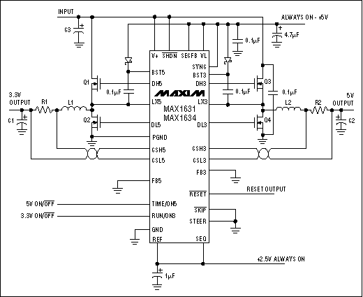
The MAX1630/MAX1633 and MAX1632/MAX1635 ICs each contain 12V/120mA linear regulators in addition to the 5V and 3.3V regulators. In place of 12V regulators, the MAX1631/MAX1634 devices accept feedback from a transformer secondary and provide a control pin that selects which regulator (3.3V or 5V) receives the secondary-feedback signal. This signal aids in the generation of auxiliary voltages other than 12V. Coupled via an external resistor divider, it adjusts the point of voltage regulation for the secondary winding. A simplified application circuit, containing no transformer and therefore producing only two output voltages, is shown in Figure 1.

Figure 1. This standard application circuit features a second-generation multi-output step-down DC-DC converter IC.
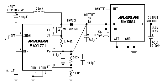
MAX1633-MAX1635 ICs, which lack the under- and overvoltage protection internal to MAX1630-MAX1632 devices, are intended for use in troubleshooting prototype boards, and also for use in applications for which the supply voltages are held up by keep-alive supplies, which can otherwise interfere with overvoltage-protection circuitry. Two-Regulator Step-Up ConfigurationsOne of the two-regulator step-up topologies employs a switching regulator to step up to 5V and a linear regulator to step back down from 5V to 3.3V (Figure 2). This circuit offers simplicity in exchange for efficiency. Step-up efficiency is generally less than step-down efficiency, and the overall conversion from input to 3.3V equals the 5V regulator's step-up efficiency times 66% (output over input for the linear regulator times 100).

Figure 2. This combination produces 5V and 3.3V regulated outputs by stepping up with a switcher and down with a linear regulator.
You can improve this conversion efficiency by replacing the linear regulator with another switching regulator, which steps up from VIN to 3.3V, but the penalty is an increase in cost, output noise, and board area. In lighter-load applications, note that a MAX866 step-up switching regulator can be substituted for the MAX1771 to allow startup from lower voltages, as from a single-cell battery. Because the minimum startup voltage is a function of load current, you must test for this parameter at the maximum intended load. The MAX866, for instance, guarantees a startup voltage of no more than 0.9V at no load and 1.2V typical (not guaranteed) at 20mA.
To enable startup with the minimum-possible supply voltage, engineers sometimes arrange to connect the load only after the regulator has started. After startup, a step-up switching regulator in the bootstrapped configuration is capable of running on supply voltages lower than its minimum-allowed startup level. This behavior benefits battery-powered systems that run continuously; they start up easily when the battery is fresh and continue to operate as the battery voltage declines well below the minimum startup level. The MAX866, for example, continues to deliver 20mA while the input can decline to 1.0V. For heavier load currents at the cost of higher startup voltages, consider the MAX1771 or the MAX856 family of regulators.
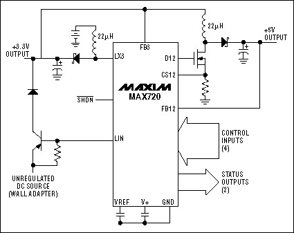
Finally, Maxim offers a dual-voltage step-up regulator that produces both 3.3V and 5V with a moderate output-current capability (Figure 3). Its main switcher generates 3.3V with an IOUT capability (800mA maximum) that is proportional to the input voltage. The auxiliary 5V supply, which requires an external MOSFET and sense resistor, has a maximum allowable output current that depends on VIN, the current-limit resistor, and other external components.

Figure 3. A single-IC dual-output step-up switching regulator produces 3.3V and 5V outputs.
The MAX720 not only operates from the output of an optional wall-cube supply; by monitoring the wall-cube connection, it extends battery life by shutting down the main 5V supply when wall-cube power is available. Also provided is a shutdown mode that disables both switching supplies, subject to an override when the linear regulator is operating (usually via power from a wall cube).
A similar article appeared in the March 1996 issue of Computer Design.
欢迎分享,转载请注明来源:内存溢出

 微信扫一扫
微信扫一扫
 支付宝扫一扫
评论列表(0条)