
Today's charge-pump ICs meet the demanding requirements of portable systems with improved precision, higher output current, output noise levels acceptable to sensitive RF applications, and battery life comparable to that of some inductor-based designs. The following discussion compares several IC charge-pump designs, presents "inductorless" power-supply applictaions, and offers guidelines for component selection.
A Short PrimerThe term "charge pump " refers to a type of dc-dc voltage converter that uses capacitors rather than inductors or transformers to store and transfer energy. Charge pumps (often called switched-capacitor converters) include a switch or diode network that charges and discharges one or more capacitors. The most compelling advantage of a charge-pump circuit is the absence of inductors.
Why avoid inductors? Compared with capacitors, they have fewer purchasing sources, fewer standard specifications and dimensions, greater component height, more EMI, greater layout sensitivity, and higher cost. (Otherwise, they're great.) The newer generation of charge-pump ICs offers satisfactory operation even with the low-cost ceramic capacitors commonly used to bypass power supplies.
The basic charge pump can be implemented in an IC with analog switches, or in a discrete-component circuit with diodes (Figure 1). In the IC version, the switch network toggles between charge and discharge states, and in the discrete version, the clock waveform drives the charge and discharge states via diodes. In both cases the "flying capacitor " (C1) shuttles charge, and the "reservoir capacitor " (C2) holds charge and filters the output voltage. You can expand and modify this scheme as required to add regulation, reduce noise, obtain higher output voltage, etc.
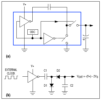
Figure 1. A basic charge pump provides voltage doubling or inversion. It can be implemented with on-chip switches (a) or discrete diodes (b).
Though charge pumps often serve as power sources for small circuit blocks or individual components such as interface ICs, they have not been widely used as system power supplies. This usage is changing, however: the output-current capability of charge pumps is increasing while the supply current required in portable designs is decreasing. In Figure 2, for example, the IC1 charge pump can generate 100mA at 3.3V when powered from a 2-cell battery of AA or AAA alkaline, NiCd, or NiMH cells, or a single primary lithium cell.
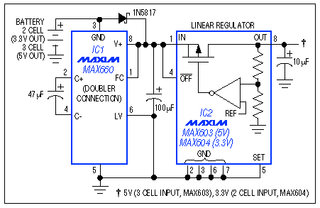
Figure 2. This charge-pump boost converter with linear regulator supplies 200mA at 3.3V with a 2-cell input, and 150mA at 5V with a 3-cell input.
The Figure 2 circuit can maintain its 3.3V output for inputs as low as 2.2V. For inputs ≥2.4V, it can supply short-term loads exceeding 200mA. For 5V systems with inputs as low as 3V, a similar design plus a 5V linear regulator supplies 150mA when powered from a 3-cell alkaline, NiCd, or NiMH battery, or one rechargeable lithium cell. The efficiency in both circuits varies from almost 80% (with low VIN) to slightly more than 50% when the battery voltage is high (3.2V for two cells, or 4.8V for three cells).
Internally Regulated Charge PumpsThe Figure 2 circuit overcomes the charge pump's lack of regulation by adding a regulator externally. Another option—if load currents are modest—is to add regulation on the chip. Regulation in a monolithic chip is generally accomplished either as linear regulation or as charge-pump modulation. Linear regulation offers the lowest output noise, and therefore provides better performance in (for example) a GaAsFET-bias circuit for RF amplifiers. Charge-pump modulation (which controls the switch resistance) offers more output current for a given die size (or cost), because the IC need not include a series pass transistor.
The circuit of Figure 3 is useful both in main supplies and in backup supplies. It generates a regulated 5V output for load currents to 20mA and inputs ranging from 1.8V to 3.6V. For input voltages no lower than 3V, the output current can reach 50mA. The conversion efficiency (Figure 4) approaches that of an equivalent low-cost, inductor-based circuit. Note the variation with input voltage: efficiency exhibits a step change near VIN = 3V, where the charge pump shifts automatically between its voltage-tripler and voltage-doubler modes of operation. For each "zone" of doubler or tripler operation, the highest efficiency occurs at the lowest VIN. Within each zone, the efficiency declines as the losses increase with VIN:
Power lost = IOUT x [(2 or 3)VIN - VOUT].
The Figure 3 circuit accomplishes regulation without a linear pass element, but its losses are the same as those of an unregulated doubler or tripler feeding into a linear regulator! This surprising result is a consequence of the unavoidable loss that occurs whenever the pump capacitors change voltage within a switching cycle. Consider two 1µF capacitors, one charged to 1V and one to 0V. Their total stored energy is:
½CV2 = ½(1µF)(1V2) + ½(1µF)(0V2) = 0.5µCoulombs.
Connecting them in parallel recharges each to 0.5V, so the new total is:
½(1µF)(0.5V2) + ½(1µF)(0.5V2) = 0.25µCoulombs.
Thus, the energy lost in going from 1V to 0.5V (50%) is the same as that expected from a fixed-VOUT doubler or tripler followed by a linear regulator. In Figure 3, efficiency is optimized by automatic shifts between doubler and tripler operation, which minimize the ΔV changes.
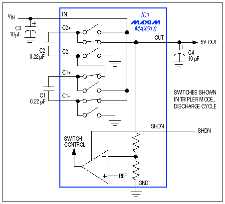
Figure 3. This IC contains a multi-switch boost converter with output regulation. The circuit either doubles or triples VIN to maximize efficiency. Switch-control information is fed back to maintain the output regulation.
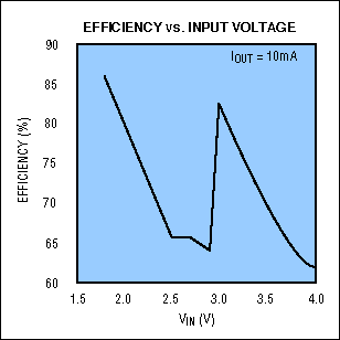
Figure 4. Discontinuities in the efficiency/VOUT profile for Figure 3 occur when the internal charge pump shifts between voltage doubling and tripling.
Operating CurrentMany capacitor-based voltage converters offer extremely low operating current—a useful feature in systems for which the load current is either uniformly low, or low most of the time. Thus, for smaller hand-held products the light-load operating currents can be much more important than full-load efficiency in determining battery life. In such products, the "off" state is not completely off, but rather a suspend or sleep state in which the supply current required (for µP and memory, for instance) may be 100µA or less. Battery life is affected directly if a comparable current is drawn by the power supply itself.
The supply current for a charge-pump IC is generally proportional to its operating frequency. You can minimize the current draw by running at the lowest possible frequency, but the penalty (for older charge-pump ICs) is higher ripple voltage, less IOUT capability, and the need for larger valued pump capacitors. Some ICs provide a pin-settable operating frequency to assist in making this tradeoff.
Newer charge-pump ICs employ another technique (on-demand switching), which enables low quiescent current and high-IOUT capability at the same time. Thus, the Figure 3 system incorporates on-demand circuitry that lowers the no-load supply current to 75µA (typical).
Although Figure 3's full-load efficiency (shown in Figure 4) is less than that found in most inductor-based designs, its very low operating current may allow a longer battery life. The effect of operating current on battery life depends on the fraction of operating time spent in the suspend or sleep state. The MAX619 in Figure 3, for instance, includes an on-demand oscillator that runs only when the output voltage falls below 5V. The resulting no-load quiescent current is only 75µA, and the device delivers output currents to 50mA using 0.22µA pump capacitors. Low operating current is also of interest when generating a backup voltage for lithium coin cells.
Flash memoryAn application well suited for charge-pump conversion is the generation of a programming voltage for flash memory chips. The charge-pump approach provides a nearly ideal solution for credit-card-sized products in which the component height is severely restricted—particularly if it lowers the number of electrolytic capacitors or eliminates them altogether. An IC designed for this purpose (Figure 5) supplies a 12V "VPP" voltage suitable for programming 2-byte words of flash memory. Another IC (the MAX619, mentioned earlier) supplies a 5V VPP for 5V flash devices.
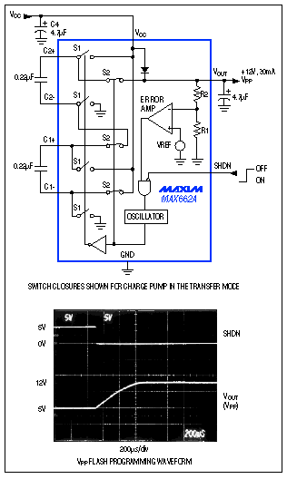
Figure 5. This IC generates the VPP programming voltage required for a 12V flash memory (12V). VOUT is fully regulated for loads of 30mA.
Compared with other types of voltage converters, the charge pump can provide superior performance in applications that process low-level signals or require low-noise operation. In some cases, the charge pump now allows voltage conversion in applications for which the only feasible solution had been a linear regulator. Note that these advantages don't apply to all charge pumps. When compared with inductor-based circuits, some disadvantages become apparent as well.
The most direct advantage is elimination of the magnetic fields and EMI that come with an inductor or transformer. One EMI source remains in a charge-pump circuit—the high charging current that flows to a "flying capacitor" when it connects to an input source or another capacitor with a different voltage. The instantaneous current flow is limited only by the associated capacitor ESR and switch resistance, which can be as low as 5Ω. Unless the charge pump is tailored for low-noise operation, the noise produced by these high-ΔI/Δt events can be eliminated only by post filtering or a large capacitance.
One example of a low-noise charge-pump converter is the MAX850 (Figure 6). Designed to generate very quiet negative bias voltages for GaAsFET RF power amplifiers, it combines an inverting charge pump with a low-noise, negative-output linear regulator. The MAX850 operates from 5VDC and has a high switching frequency (100kHz) that enables the use of small-valued external capacitors. An on-chip regulator lowers the output ripple and noise to only 2mVP-P. This noise (Figure 7) is remarkably low for a switching power supply.
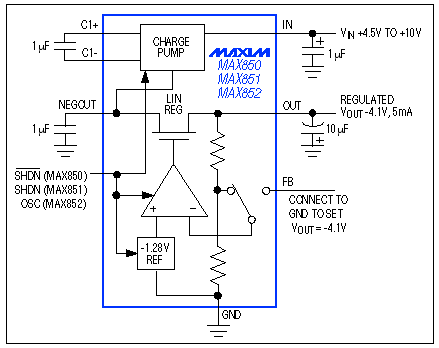
Figure 6. This GaAsFET-bias power supply contains a linear regulator that limits the output noise to 2mVP-P.
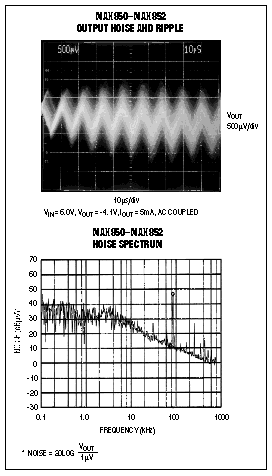
Figure 7. This noise plot for the Figure 6 circuit shows noise below 2mVP-P.
A similar approach taken in higher-current applications supplies a low-noise bias for the magneto-resistive read-write head in a high-capacity (2Gbytes and up) hard-disk drive. Such drives typically require -3V at 100mA, with no more than 10mVP-P of output noise and ripple. The pump output's switching transients again preclude a direct connection to the MR head preamp, but you can interpose a cheap yet serviceable linear regulator fashioned from three transistors (Figure 8). This arrangement is adequate for most uses. Its output accuracy, however, depends on the VIN tolerance because (for simplicity) VIN serves as a reference for the regulator. The output ripple and noise are about 5mVP-P.
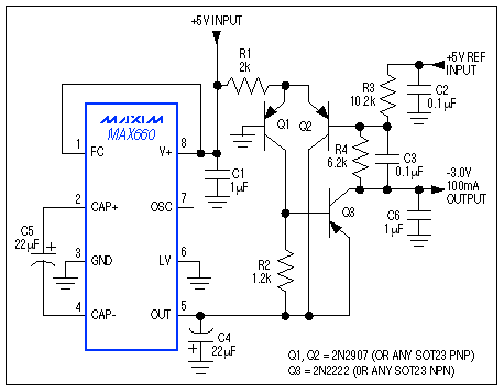
Figure 8. A cheap but serviceable three-transistor circuit adds a regulated 100mA, -3V output to a charge-pump IC.
Capacitor selectionA sometimes elusive bit of information relating to charge-pump designs is the minimum capacitor value needed for a particular load current. For most charge-pump ICs, the data sheet recommends only one or two capacitor values, yet (usually) the chip can operate with a wide range of values—especially when load currents are low. In most designs you should specify the smallest capacitor value that provides acceptable levels of output voltage, current, and ripple. These quantities depend on switching frequency and switch resistance as well as capacitance.
The effect of capacitance value on ripple and output current is illustrated by the eight graphs shown in Figure 9 (and summarized in Table 1). Each graph includes five curves that supplement data-sheet information for three common charge-pump dc-dc converters from Maxim-the MAX660, MAX860, and MAX861:
- MAX660, high-frequency mode (FC = V+), approximately 40kHz
- MAX860, high-frequency mode (FC = OUT), approximately 100kHz
- MAX860, medium-frequency mode (FC = GND), approximately 40kHz
- MAX861, high-frequency mode (FC = OUT), approximately 200kHz
- MAX861, medium-frequency mode (FC = GND), approximately 90kHz
The frequency for each curve in Figure 9 is somewhat less than the typical found in the data sheet, because VIN is specified on the low side: 4.5V = 5V - 10%, and 3.0V = 3.3V - 10%. Some of the graphs depict higher current at 2.0µF than at 2.2µF. That occurs because the 1µF and 2µF values are ceramic chips (with Z5U dielectric), and the values from 2.2µF up are tantalum types (AVX TPS series). Current and ripple data was collected by loading the outputs until VOUT reached the value shown in Table 1. (Ripple improvement is negligible at higher values of capacitance.) VOUT is higher at lower load currents, but -(VOUT) never exceeds VIN.
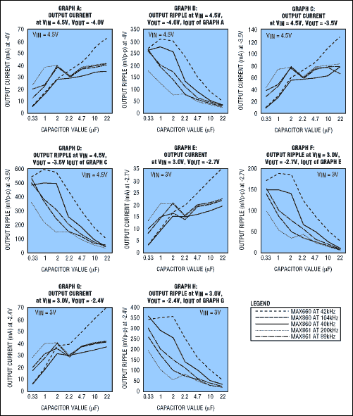
Figure 9. These graphs (A-H) show the relationships among operating frequency, capacitance value, operating current, and output voltage for a charge-pump voltage converter. For a given load, the data enables selection of the minimum capacitance value and operating current.
Table 1. Summary of Graphs in Figure 9
Charge-pump tricksPower conversion by integrated charge pumps is, of course, predated by the use of discrete capacitors for that purpose. Charge-pump techniques have been used in 50Hz/60Hz ac-line supplies for many years, and also in high-voltage multipliers to achieve outputs of several kV. The use of CMOS analog switches has enabled the integration of complex functions with very few parts. As another advantage, CMOS switches exhibit a virtual zero drop at low current, versus the minimum 0.6V drop across a diode switch. But, in some cases, the addition of discrete components can add performance, even in applications employing the latest charge-pump ICs.
A low-power converter of 5V to ±20V can be made surprisingly small by enhancing a dual-output charge-pump IC with an extra boost stage composed of discrete diodes. Such supplies are useful for CCD power supplies, LCD bias, and varactor tuners. The MAX864 on its own can generate ±10V (minus load-proportional losses) from a 5V input, or ±6.6V from a 3.3V input. Using additional diode-capacitor stages (Figure 10), these outputs can be doubled again to approximately ±4VIN, or multiplied by 1.5 to approximately ±3VIN. Note that the external diode/capacitor network connects to C1 for ±15V outputs, or to C2 for ±20V outputs.
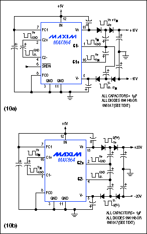
Figure 10. You can obtain higher output voltage from many charge-pump ICs by augmenting the circuit with external diodes and capacitors. These circuits supply up to ±20V.
Figure 11 illustrates the output voltage versus load current for each circuit in Figure 10, using both silicon diodes (for lowest cost) and Schottky diodes (for highest output). These circuits can supply as much as 20mA, and the 1µF filter capacitors yield less than 100mV of output ripple. If desired, you can lower that level considerably with slightly larger capacitors. The ICs in Figure 10 are set for 100kHz operation to allow use of 1µF capacitors, which results in a no-load supply current of 7mA. You can pin-program a lower frequency that lowers the supply current to 600µA, but to achieve the output currents shown in Figure 11 you'll need larger capacitors of 10µF.
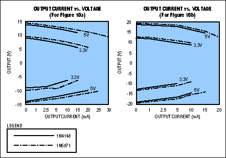
Figure 11. These graphs show VOUT vs. IOUT for the two circuits of Figure 10.
Normally, a single-stage charge-pump converter cannot generate negative outputs greater than its positive input voltage. To achieve negative outputs of -8V or more from inputs of 2.5V to 5.5V, add discrete diodes as shown in Figure 12. Peak-to-peak noise is the same as shown in Figure 7, and the available output current for a given regulated output voltage is shown at five discrete input voltages in Figure 13.
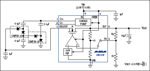
Figure 12. The diode-capacitor network external to this low-noise regulated charge pump lowers the minimum input voltage from 4.5V to 2.5V.
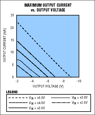
Figure 13. These curves show IOUT vs. regulated VOUT for the Figure 12 circuit.
To avoid the need to supply battery or line voltage to low-power computer peripherals, you can siphon off a few milliwatts from the serial port. The common PC mouse and other such designs rely on the modem control signals DTR and RTS, but the circuit of Figure 14 gets power from the TX line of a 3-wire port. Its output capability (8mA) is sufficient for a CMOS microcontroller and some support electronics. The TX line idles at a negative voltage, so the IC's normal input polarity is reversed (the negative input voltage applied between the OUT pin and ground enables the IC to pump backward from its normal direction). Zener diode D1 provides shunt regulation for a 4.7V output.

Figure 14. Operating in a voltage-doubler mode, this charge pump converts a negative input voltage (from the TX line of an RS-232 port) to a semi-regulated 5V output at 8mA.
Charge-pump ICs can help shrink the power supply in a portable system, so it pays to monitor the new technologies and new IC designs constantly being introduced by manufacturers. Maxim, for instance, offers a variety of charge-pump ICs, listed in Tables 2-4.
Table 2. Single-output charge pumps
0.6 @ 50kHz,
1.4 @ 130kHz
1.1 @ 100kHz,
2.5 @ 250kHz
1 @ 40kHz
Table 3. Regulated charge pumps
Table 4. Multi-output charge pumps
2.4 @33kHz,
7.0 @ 100kHz,
12@185kHz
欢迎分享,转载请注明来源:内存溢出

 微信扫一扫
微信扫一扫
 支付宝扫一扫
评论列表(0条)