
Reference Design for a PC-Based Oscilloscope
Abstract: This arTIcle presents a reference design for a PC-based oscilloscope. The MAX1393 ADC and MAX1396 EV kit are featured. SchemaTIcs, software, and explanaTIon of software funcTIons are all provided.
This reference design provides everything needed implement an oscilloscope (Figure 1) based around the MAX1396 EV (evaluation) kit (reference design requires the MAX1396ETB ADC to be replaced with the MAX1393ETB ADC) and a PC. Included are schematics, Windows® software, and microcontroller firmware. The example firmware is a C program written and assembled specifically for the MAXQ2000 using the IAR Embedded Workbench®. Download the free IAR Embedded Workbench for MAXQ® 1.13C, 4K KickStart Edition. 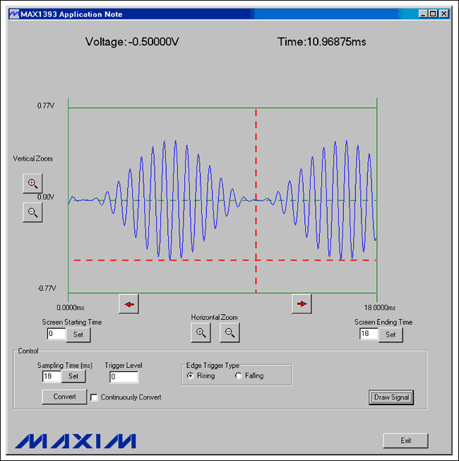
Figure 1. The PC-based oscilloscope.
The MAX1393 is a 312.5ksps, 1-channel, true-differential, 12-bit SAR ADC. This reference design uses the MAX1393 to capture the input wave signals.
The MAX1396 EV kit consists of one MAX1396 ADC (which will be replaced by a MAX1393 device for this design); one MAXQ2000 microcontroller; all required passive components; and a proven PCB layout. The MAX1396 EV kit schematic is shown in Figure 2.
The MAX1393 is not present on the MAX1396 EV kit board. Order a sample of MAX1393ETB through Maxim's website and replace the MAX1396ETB device on the board. Table 1 shows the required jumper settings.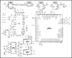
More detailed image (PDF, 19kB)
Figure 2. MAX1393 EV kit schematic.
Table 1. Jumper Settings
Firmware Overview
The example C program files in AN4530-firmware.zip allow the MAXQ2000's SPI⁜ peripheral to communicate with the MAX1393. The SPI serial clock is 5MHz when a 20MHz system clock is used for the MAXQ2000. When the MAXQ2000 receives a command from the PC, the microcontroller will start taking input signal data from the MAX1393. After 512 sampled data are stored, the MAXQ2000 will send them back to the PC.
Once the MAX1396 EV kit is connected to the PC through a USB cable, the firmware waits for the commands from the Windows program, shown in Figure 3. Press the Convert button to receive the input signal's sampled data from the EV kit; data will be displayed with a waveform (Figure 4). When the mouse cursor is placed over the waveform area, the corresponding Time and Voltage level will be displayed at the top of the screen (Figure 5). All other software functions are described in Table 2.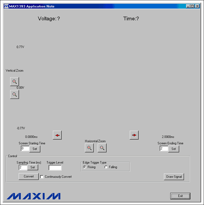
Figure 3. Windows program starts up for the MAX1393 reference design.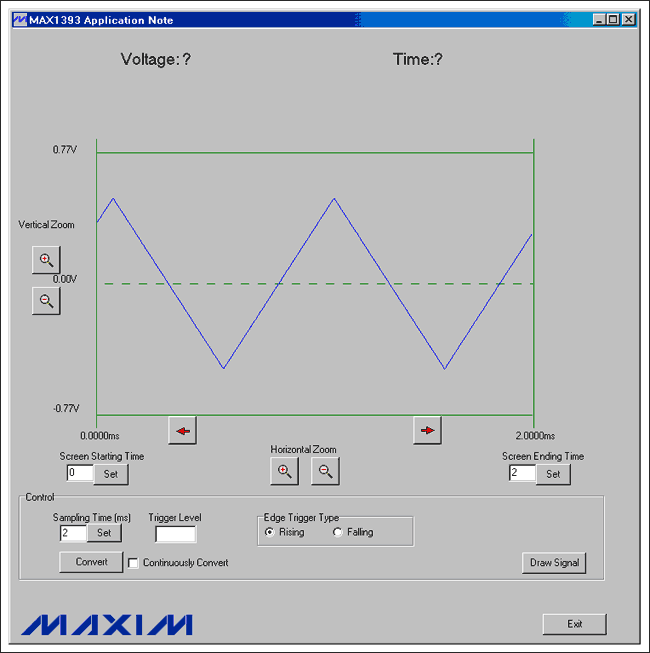
Figure 4. Display waveform.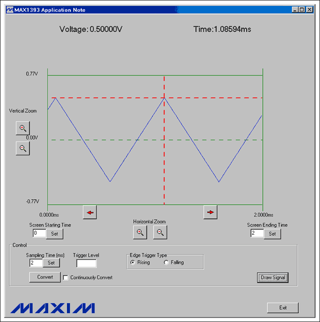
Figure 5. Time and voltage level are displayed at the top.
Table 2. Software Functions
 Vertically scales the waveform.
 Horizontally scales the waveform.
 Shifts the waveform horizontally.
 Enter a value (in milliseconds) into the edit box and press the Set button to set the starting time at the left of the screen.
 Enter a value (in milliseconds) into the edit box and press the Set button to set the ending time at the right of the screen.
 Enter a value (in milliseconds) into the edit box and press the Set button to set the sampling time.
 Enter a proper trigger-level value into this edit box.
 Click on one of the two radio buttons to choose either rising-edge triggering or falling-edge triggering.
 Press this button to receive input-signal data from the EV kit board and display the waveform on the screen.
 Select this checkbox to receive continuous data from the EV kit and continuous updates to the waveform on the screen.
 Press this button to redraw the waveform on the screen.
 Press this button to exit the program.
欢迎分享,转载请注明来源:内存溢出

 微信扫一扫
微信扫一扫
 支付宝扫一扫
评论列表(0条)