IntroducTIonThis applicaTIon note shows a how to connect a Dallas BERT to a Dallas framer/single-chip transceiver (SCT). This applicaTIon note applies to the following products:

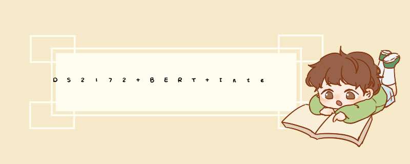
Figure 1. Framer/SCT to DS2172/DS21372 interface.
The RCHBLK and TCHBLK outputs from the framer/SCT are used to determine the time slot or band in which the BERT is to transmit or receive data. These pins are programmed using the RCHBLK/TCHBLK registers. The RCHBLK/TCHBLK pins are normally low; writing the register bits to one will set the pin to a high voltage during that time slot. In this configuration, setting the RCHBLK and TCHBLK pins high enables the DS2172/DS21372 to transmit and receive data.
Figure 1 shows the DS21x5y with the elastic stores disabled. If the elastic stores are enabled, the user will use the system clock (TSYSCLK, RSYSCLK) as inputs to the DS2172/DS21372 rather than RCLK and TCLK.
Note: In T1 framers/SCTs, the TCHBLK/RCHBLK pin cannot be configured to be high during the F-bit position. This means the DS2172/DS21372 cannot source data during the F-bit position of each frame. E1 framers/SCT TCHBLK/RCHBLK can be programmed to be high during the entire frame. Listed below are the TCHBLK/RCHBLK registers for any E1 framer or any E1-only SCT listed above.
RCBR1/RCBR2/RCBR3/RCBR4: Receive-Channel Blocking Registers
(2B to 2E Hex) (MSB) (LSB)
0 = force the RCHBLK pin to remain low during this channel time
1 = force the RCHBLK pin high during this channel time
TCBR1/TCBR2/TCBR3/TCBR4: Transmit-Channel Blocking Registers
(22 to 25 Hex) (MSB) (LSB)
0 = force the TCHBLK pin to remain low during this channel time
1 = force the TCHBLK pin high during this channel time
Listed below are the TCHBLK/RCHBLK registers for any T1 framer or any T1-only SCT listed above.
RCBR1/RCBR2/RCBR3: Receive-Channel Blocking Registers
(6C to 6E Hex) (MSB) (LSB)
0 = force the RCHBLK pin to remain low during this channel time
1 = force the RCHBLK pin high during this channel time
TCBR1/TCBR2/TCBR3: Transmit-Channel Blocking Registers
(32 to 34 Hex) (MSB) (LSB)
0 = force the TCHBLK pin to remain low during this channel time
1 = force the TCHBLK pin high during this channel time
If you have further questions about connecting any of our framers/SCTs to our BERTs, then please contact the Telecommunication Applications support team via email [email protected] call 972-371-6555.
Dallas Framer/SCT And BERT Information
欢迎分享,转载请注明来源:内存溢出
 微信扫一扫
微信扫一扫
 支付宝扫一扫
评论列表(0条)