DescripTIonThis applicaTIon note is intended to show how to interface a user-defined device-under-test (DUT) or development board with the DST1E1DK SCT Design Kit. The DST1E1DK development board was designed by Dallas Semiconductor to facilitate user tesTIng and prototyping of Dallas Semiconductor single-chip transceivers (SCTs). These boards feature an 8051 processor-based microcontroller, on-board EPROM, a socket for testing different Dallas Semiconductor SCTs, and a DS2172 Bit Error Rate Tester (BERT). In addition to these features, the board offers a prototyping area and expansion ports. The focus of this application note is to show how an expansion port can be used to expand the development board functionality to include testing of user-defined devices or complete boards, giving the user virtually unlimited testing flexibility.
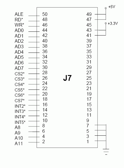
Expansion Port DefinitionThere are two expansion ports labeled J7 and J10 on the DST1E1DK boards. The focus of this application note will be J7. Expansion Port J7 provides user access to an 8-bit, microprocessor-multiplexed address/data bus, four more most significant address bits, the Address Latch Enable (ALE), the microprocessor read and write signals ( active-low RD and active-low WR , respectively), six different chip selects, and four separate interrupts. Additionally, it provides access to the 5V, 3.3V, and ground planes. A pinout for Expansion Port J7 is shown in Figure 1.
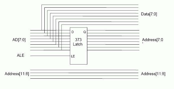
For most user applications, microprocessor bus access will be necessary. For instance, if the user wishes to have read and write access to registers in the DUT or target board, that access is accomplished via this bus. If separate address and data lines are needed, the multiplexed bus can be demultiplexed fairly easily with the use of a latch, such as a 74HC373. A sample diagram is shown in Figure 2.
Once the address and data lines are demultiplexed, the user will have all signals necessary for a standard processor interface, namely address, data, chip select, and read and write strobes. As is standard with Intel based bus architectures, active-low CS , active-low RD , and active-low WR strobes are active low. The 373 latch will serve to hold the address lines stable when LE is low. For target reads, data can then be driven onto the bidirectional address/data bus by the DUT as indicated by the active-low RD pulse. For target writes, data will be driven onto the address/data bus by the processor after the address bits have been latched via ALE, providing both stable address and data at the time of the active-low WR strobe. Please refer to the 8051-processor-family data sheets for more detailed information regarding timing and bus characteristics.
The chip-select signals are generated by a standard 3-8 decoder on the DST1E1DK board using the upper most address bits [14:12]. Chip Select 0 is used to access the SCT on the DST1E1DK board, while Chip Select 1 is used to for accesses to the DS2172 BERT chip on the DST1E1DK board. The user can then choose from any of the six remaining chip selects. Since these chip selects are generated from the three most-significant-address bits, these traces are not brought out to the expansion port.
DEF File ModificationIn order to define the memory map of any user-added DUT or board that is interfaced with the DST1E1DK board, the user must modify the supplied DEF files to include links to the DEF file for the user DUT or interfaced board. A DEF file is simply a file that defines the memory map of the system for the development software, including information such as register names, addresses, bit definitions, and display format. If more than one device is to be interfaced, than multiple links will have to be made to the base DEF file. For general information on DEF file format and usage, please refer to the literature included with the DST1E1DK design kit. When the user purchases this development kit, several DEF files are included for use with the base T1E1DK board. These include a DEF file for the DS2172 BERT chip, as well as DEF files for the various SCTs that can be used in the socket. In order to let the software recognize the newly added DUT or user defined board, these supplied files must be modified to include a LINK to the user created DEF file, which defines the users memory map and base offset. The OFFSET listed in the users DEF file must correspond to the chip select that the user wishes to employ. For Chip Select 2, for example, the user would define the OFFSET in the DEF file as 0x2000h. For Chip Select 3, the OFFSET would be 0x3000h, and so forth. Once this file is created and linked to the DEF file for the SCT on the base board, the user will be able to access their registers via the DST1E1DK software, just like the registers sets in the BERT chip or the SCT being used.
SummaryInterfacing user-defined devices to the DST1E1DK is an easy and potentially robust way to create development platforms. The Dallas Semiconductor board provides a simple processor interface and development software as well as multiple SCTs and a DS2172 BERT chip for the end user to build off of or interface to. The development board provides easy access to all necessary traces, either via the two expansion ports or via standard header interfaces, allowing the user to jumper between the Dallas Semiconductor board and the DUT. With the ability to choose between multiple SCTs, the processor, and the BERT chip, the user can test virtually any telecommunication device or product.

Figure 1. J7 Expansion Port.
*denotes active-low signal.

Figure 2. Simple Latch Diagram For Demultiplexing The Address/Data Bus.
欢迎分享,转载请注明来源:内存溢出

 微信扫一扫
微信扫一扫
 支付宝扫一扫
评论列表(0条)