IntroductionThis application note applies to the following products:
In a SLC-96-based transmission scheme, the standard Fs-bit pattern is robbed to make room for a set of message fields. The SLC-96 multiframe is made up of six D4 superframes, so it is 72 frames long. In the 72-frame SLC-96 multiframe, 36 of the framing bits are the normal Ft pattern and the other 36 bits are divided into alarm, maintenance, spoiler, and concentrator bits, as well as 12 bits of the normal Fs pattern. Please see the Bellcore document TR-TSY-000008 for more details about SLC-96.
Receive-Side SLC-96 ApplicationsTo enable the device to synchronize onto a SLC-96 pattern, the following configuration should be used:
- Set to D4 framing mode (CCR2.3 = 0)
- Set to cross-couple Ft and Fs bits (RCR1.3 = 1)
- Set to minimum sync time (RCR1.2 = 0)
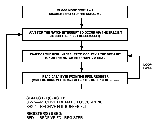
Figure 1 describes the method used to extract the SLC-96 message bits. The devices contain an on-board SLC-96 synchronizer that is enabled when the CCR2.1 bit is set to one. In this mode, the match flag (SR2.2) takes on a new meaning; it will indicate when the framer has received the 12-bit Fs pattern that exists in SLC-96 multiframe. In each SLC-96 multiframe, the user will read the RFDL register three times. The external controller will wait for the match flag to be set. Once set, the controller will then wait for the RFDL to fill.

Figure 1. SLC-96 Message field extraction via RFDL.
Figure 2 details how the SLC-96 fields will be represented in the RFDL register on each read. Since the RFDL is also used in the ESF framing mode, the zero destuffer should be disabled (CCR2.0 = 0). (Note: The match registers (RFDLM1 and RFDLM2) are not used in SLC-96 mode and can be programmed with any value.)

Figure 2. RFDL Register byte sequence.
Transmit-Side SLC-96 ApplicationsTo insert the SLC-96 message fields, the user has the option to either use the external TLINK pin or to use the onboard TFDL register. Usage of the TLINK pin will require some external hardware and to enable this option, the TCR1.2 bit should be set to one. This application note concerns itself solely to the use of the TFDL register to insert the SLC-96 message fields.
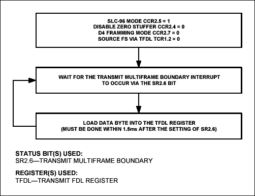
Figure 3 displays the method to enable the device to insert the SLC-96 message fields via the TFDL register. On each normal D4 multiframe boundary, the framer will signal to the user via the SR2.6 bit to write to the TFDL the sequence of bytes shown in Figure 4. The user will write to the TFDL six times in each SLC-96 multiframe.

Figure 3. SLC-96 Message field insertion via TFDL.

Figure 4. TFDL Register byte sequence.
T1 Framer And Single-Chip Transceiver InformationFor more information about Dallas Semiconductor's T1/E1 framers and single-chip transceivers, please consult the data sheets available on our website at www.maxim-ic.com/telecom.
If you have further questions concerning the operation of Dallas Semiconductor's T1/E1 framers and single-chip transceivers, please contact the Telecommunication Applications support team via email [email protected] or call 972-371-6555.
欢迎分享,转载请注明来源:内存溢出

 微信扫一扫
微信扫一扫
 支付宝扫一扫
评论列表(0条)