
This application note defines common-mode signals and common-mode-rejection (CMR), describes how high-common-mode transceivers are able to handle ±50V ground-offset signals, and indicates how the limits on offset voltage and frequency are affected by the use of shielded or unshielded data-transmission lines. A method of transferring power across the isolation barrier is explained, and fail-safe and protection circuits are discussed.
The application uses the MAX3157 high common-mode-rejection RS-485 transceiver. This device provides a ±50V isolated data interface and power for the line-side transceiver circuits. Unlike optically-isolated or transformer-isolated RS-485 transceivers, its main features are low cost, an allowed ±50V resistive-isolation character in a single small IC package, and capacitive power transfer from non-isolated to isolated-side circuitry. It operates from a single +5V system-power source, and requires only three small external capacitors for operation. An overall low profile is maintained when compared to other isolation techniques requiring opto-couplers and/or a transformer.
Pseudo-Isolated RS-485 TransceiverFigure 1 shows the MAX3157's isolation, power-transfer, and protection circuits.
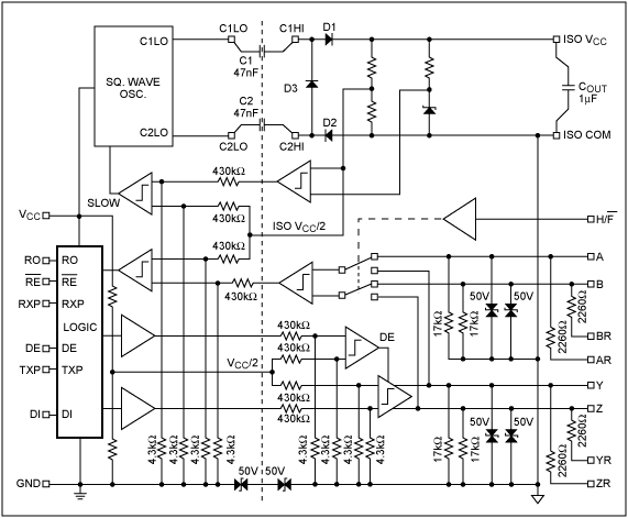
Figure 1. The MAX3157 functional block diagram.
Common-Mode DefinitionThe definition of common-mode voltage (VCM) when related to a two-wire transmission cable is taken to be the average of the two signal voltages in relation to the local ground. This can be represented mathematically as

This definition is represented graphically in Figure 2 where a 3V differential-mode signal is riding on a 2.5V common-mode signal. The offset is typical of differential-mode transmitters operating from a single supply.
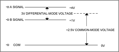
Figure 2. Representation of common-mode DC offset voltage of typical RS-485 transmitter.
As RS-485 cables may be quite long, it can happen that the originating signal common or ground may not be at the same electrical potential as that of the receiving-location ground. The RS-4851 specification calls for connecting the drive-circuit common to the frame ground either directly or through a 100Ω resistor. Hence, the situation illustrated graphically in Figure 3 may exist. The ISO COM will take on a common-mode voltage equal to the vector sum of the ground-potential difference, the driver-offset voltage, and any longitudinally-coupled noise voltage generated along the signal path between transmitter and receiver.

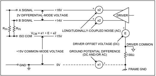
Figure 3. Common-mode voltages in two-wire line data-transmission system.
The receiving-location ground potential may differ substantially from the potential at the driver-location, and it is the difference between the two (VCM) that is of interest when considering application of the MAX3157. This VCM must be isolated from the logic side of the MAX3157.
How High-CMR Transceivers WorkHigh-CMR data transceivers include no truly-isolated circuits. Instead, they separate logic-side circuitry from line-side circuitry with high-value resistive attenuators as detailed in Figure 4. These attenuators are typically constructed so that only 1% of the input signal reaches the attenuator output. Consequently, only 1% of the applied isolation voltage reaches across the resistive barrier. Separate drivers sent data across the barrier in each direction where it is attenuated before being detected by comparators on each side of the barrier.
Reference voltages are also created on each side and sent across the barrier with identical 100:1 attenuation to bias the receiving comparators which then see the same CM voltage on both signal and reference lines. As the comparators read both the attenuated signal and the attenuated reference, a common-mode voltage of 50V occurring on the line would only translate to a 1/2V common-mode voltage on the output of the resistive barrier. As long as the differential receiver can accept the 1/2V CM voltage and is sensitive enough to detect 1/100th of the differential-signal input to the resistive attenuator, the system will operate correctly.
Thus, a full bi-directional signaling system is created with 100:1 barrier attenuation of all signals to allow two-way communication and a 50V difference across the resistive barrier. This is a pseudo-isolated circuit rather than a classically-isolated circuit, yet it accomplishes the isolation needed in perhaps the majority of applications.
Note that there is a resistance between ISO COM and system GND (see Figure 1) due to the existence of eight pairs of isolation resistors. The approximate parallel resistance of these eight attenuators is 54kΩ. The effects of these resistors will be discussed in later sections.
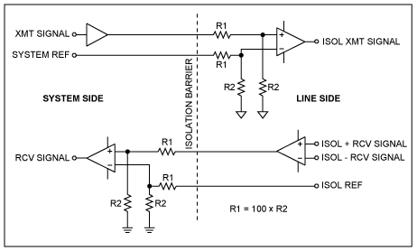
Figure 4. Resistive isolation technique.
Power Transfer Across the Isolation BarrierUnless a separate isolated power supply is available to operate the RS-485 transceiver, power must be transmitted from the system or non-isolated side to the line or isolated-side circuits without destroying the required isolation. It is a practical matter to use capacitive voltage transfer across the isolation barrier when the planned isolation is no more than 50-100V. Higher voltages can be isolated; but the required capacitors become somewhat larger at, say, 500V. Capacitive power transfer can be accomplished by differentially driving a pair of capacitors from a square-wave oscillator on the system side as indicated in Figure 5. The external capacitors feed three diodes and a filter capacitor on the isolated side to produce an isolated DC output. The third diode is present to allow recharging/discharging of the coupling capacitors on alternate half-cycles of the oscillator signal. The coupling-capacitor voltage ratings are selected to be greater than the required line-side isolation or CM voltage.
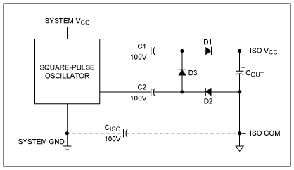
Figure 5. Capacitor-coupled isolated supply.
The isolated-supply power-transfer system operates somewhat like the well-known charge pump. The square-wave oscillator reverses its output polarity (0 or +5V) on alternate half cycles of operation. Its output is always a square wave (50% duty cycle), but (in the MAX3157) its output resistance increases on command when ISO VCC reaches its design voltage. Thus, it operates to provide either normal or reduced power transfer to the isolated supply.
As the line-side load draws down the voltage on COUT, the feedback signal will again cause the oscillator to more-effectively replenish the charge on COUT. The output voltage is thus under active regulation, with some ripple on the output at a ripple frequency depending upon the actual load. A Zener diode on the output side acts as a voltage reference against which a fraction of the output is compared to drive the control signal that is sent back across the isolation barrier to the oscillator.
The charge pump injects noise currents into the ISO COM terminal to create a noise voltage on ISO COM whenever ISO COM is not connected to system GND. Hence, for normal operation, ISO COM should be bypassed to system GND with a 10nF capacitor (CISO in Figure 5).
When ISO COM takes on a voltage from the sources shown in Figure 3, there will be a voltage divider effect due to the resistors between A and B signal inputs and ISO COM and the ≈ 54kΩ of the attenuator isolation resistors. The voltage at ISO COM will then be slightly less than the actual vector sum of e1+E+e2 shown in Figure 3.
Control and Data Transfer Across the Isolation Barrier (refer to Figure 1)Isolation is provided by the resistive isolation technique already described. Note that the data-in (DI) and driver-enable (DE) signals cross the isolation barrier from left to right or from the logic side to the line side as signals referenced to a logic-side reference voltage. The received data (RO) signal crosses the isolation barrier from right to left or from line side to logic side as a signal referenced to a line-side reference voltage. All signals, including references, are attenuated after crossing the isolation barrier by an identical amount of 1/101 or 0.99%. Each attenuated data or control signal is applied to one comparator input, and the associated attenuated reference voltage is applied to the other comparator input. The reference voltages are designed to be midway between the high and low levels of the data and control signals so that each comparator operates at maximum sensitivity.
A fourth signal crosses the isolation barrier from right to left. This is a control signal to inform the logic-side circuits that the isolated supply voltage is at its design level. This feedback control signal acts to stabilize the isolated supply voltage by asking the logic-side square-wave oscillator to increase its output resistance. As the oscillator outputs a square wave, the high-resistance mode effectively decreases the power transferred to the isolated supply.
As the circuit is designed to allow an isolation voltage up to ±50V, the attenuated maximum common-mode voltage transferred across the barrier is less than ±1/2V.
Common-Mode Isolation-Voltage LimitsThe isolation voltage limits of the MAX3157 are determined by two characteristics.
1. The charge-pump isolation-voltage limit is set by the breakdown rating of capacitors C1 and C2.
2. The data-transfer-circuitry isolation-voltage limit is set by a combination of the resistive-attenuator ratio, driver-signaling levels (related to the non-isolated and the isolated-supply voltages), differential-comparator common-mode range, and comparator signal-discrimination characteristics in the presence of noise. The specified limit for the MAX3157 is ±50V with an absolute maximum rating of ±5V. Internal back-to-back SCRs between logic and line circuits will break down when the limits are exceeded.
The rate of change of the voltage on ISO COM is unimportant to the charge pumping action as ISO VCC is essentially unaffected by rapid changes in the ISO COM voltage even with unbalanced capacitance of D1/D2 or C1/C2. Fast pulses on ISO COM will be only insignificantly reflected in the magnitude of ISO VCC in relation to ISO COM. There are, however, limitations to the magnitude and rate-of-change of the remote-ground voltage in relation to ISO COM as indicated in the following section.
Line-Interface Driver and Receiver CircuitryFor half-duplex two-wire RS-485 transmission, the internal receiver switch is set as shown; and a single 2-wire line is connected to terminals Y and Z. Transmission and reception take place in a shared manner on the single line. For full-duplex four-wire RS-422 transmission, the internal receiver switch is set to the other position where the receiver and transmitter are not interconnected. A second 2-wire line is connected to terminals A and B. Receiving and transmitting can take place simultaneously. The following discussion will treat only the RS-485 half-duplex configuration.
Typical connection between an RS-485 transceiver and the two-wire data line is illustrated in Figure 6. The second possibility, with a shielded cable, appears in Figure 7. RSHIELD may or may not be present depending upon the existence of a data-cable shield. Note that, in either shielded or non-shielded application, the cable is terminated only at both ends of the line even if there are three or more transceivers connected to the line.
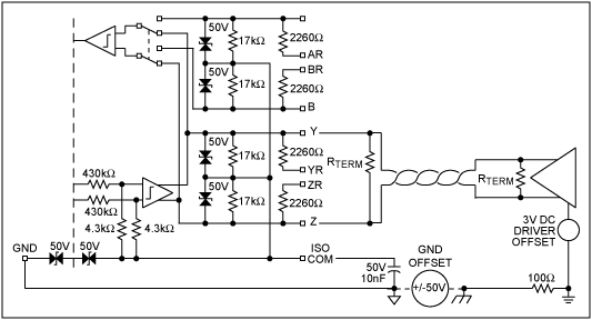
Figure 6. The MAX3157 line interface circuitry without shielded line.
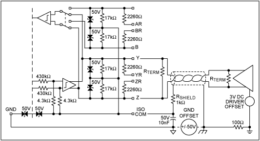
Figure 7. The MAX3157 line interface circuitry with shielded line.
RS-485 application guidelines2 call for connecting the shield to earth ground at one or both ends of the cable shield. It is recommended that the cable shield be connected to ISO COM through a 1kΩ resistor. The other end of the cable should be directly connected to earth ground per the specification. If there are MAX3157s at both ends of the cable, at least one end of the cable (and its associated ISO COM) must be connected to local earth ground. The resistor should not be of lower value than 1kΩ because it is possible, with smaller values, to set up holding currents in the MAX3157 internal SCR protection devices if the voltage on ISO COM were to exceed ±75V.
With the shield connected as shown, it is evident that the ground offset is applied to ISO COM via RSHIELD. It should also be evident that the ground offset plus the driver-offset voltage is applied to ISO COM via the receiver-input resistors. Hence, ISO COM will take on a voltage not quite equal to that of the ground offset. When ISO COM differs from logic ground, an additional voltage-divider effect occurs due to the presence of the ≈ 54kΩ parallel equivalence of the eight isolation-attenuator resistors. The voltage at ISO COM will then be slightly less than the vector sum of e1+E+e2 shown in Figure 3.
The RS-485 standard defines a 12kΩ receiver normal-mode input resistance as one unit load (U.L.) measured from either input to the receiver common (ISO COM in this example). As maximum normal-mode receiver load resistance is defined as 375Ω, thirty-two unit-load receivers may be connected to the same line. The MAX3157 contains two pairs of ≈ 17kΩ resistors internally connected between ISO COM and each of the input and output terminals A, B, Y, and Z. When the internal switch is set for RS-485 half-duplex configuration as shown, the resistors on terminals A and B are left open-circuited as these terminals are not connected. The MAX3157 is thus a bit less than a 1-U.L. device, allowing at least 32 devices to share a single line. There are two additional pairs of ≈ 2.2kΩ resistors connected, one each, to the input and output terminals A, B, Y, and Z. These resistors may be connected in parallel with the internal 12kΩ resistors by connecting terminals AR, BR, YR, and ZR to ISO COM if it is desired to create a 2kΩ (6 U.L.) receiver normal-mode input resistance.
Frequency Limits on Isolation Potential Difference, VCMThe 17kΩ receiver-input resistors reference the inputs A and B3 to ISO COM, so they will cause ISO COM to attempt to reach the mean voltage applied to inputs A and B. If there is no shield on the two-wire transmission line, ISO COM may be left unconnected except as noted below. Because of the charge pump described earlier, there is already a pair of capacitors (C1 and C2 in Figure 1) connected by circuitry from ISO COM to system GND and system VCC. These charge-pump capacitors inject about 1.4Vp-p onto ISO COM unless surpressed by a capacitor placed between ISO COM and GND. The recommended capacitor size is 10nF. A frequency-selective network is formed, as shown in Figure 8, by the combination of the receiver-input resistors between A/B and ISO COM and the isolation-attenuator resistors (REQ) paralleling capacitor CISO (and effectively C1 + C2) between ISO COM and GND. Because of this network, ISO COM will not immediately take on a DC voltage or follow an AC common-mode voltage present at the receiver inputs.
The AC common-mode voltage is most often of power-line frequency plus some content including at least the first three harmonics. A DC driver-offset voltage of ≈ 2.5V may also be present. The portion of the total signal appearing across the receiver-input resistors should not be permitted to exceed ±7Vp-p. Here it should be noted that it is not sufficient to calculate this portion of the signal by subtracting measurements made of the signal appearing on ISO COM from the measured common-mode input signal because of the phase difference between the two measured signals. Peak-to-peak measurements must be made with an oscilloscope directly between the A/B receiver inputs and ISO COM to determine this signal level (when a DC component may also be present due to driver offset). The magnitude of this signal will depend upon the methods of connection as described in Figures 6 and 7.
It is simplest to treat the unshielded-line circuit of Figure 6 first because of its relative simplicity. This also corresponds to the conditions shown in Figure 3 and in Equation 2. There are two possible cases here, either with or without terminals AR and BR connected to ISO COM. In the first case, the equivalent resistance between A/B and ISO COM is ≈ 1.1kΩ, while in the second case it is ≈ 8kΩ. This will be referenced as RIN in the following calculations. Figure 8 shows the approximate frequency-selective circuit equivalent.
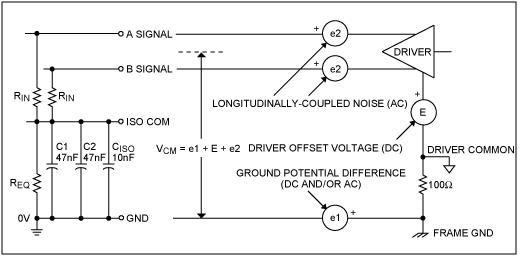
Figure 8. Equivalent input circuit for unshielded line.
When a driver-offset voltage is present on the unshielded cable (Figure 8), this offset will be distributed across RIN and REQ as if e1 and e2 were not present. About 2% of EOFFSET will be present across RIN when terminals AR and BR are connected to ISO COM, and about 13% when not connected. The typical EOFFSET of 2.5V may then be safely ignored in most cases when evaluating the limits on AC valued e1 + e2 due to the relatively high value of REQ. If it is desired to calculate the fraction of e1 and e2 appearing across RIN, Equation 3 may be used to determine the effect of the fundamental frequency content. Note that (e1 + e2) is a vector sum.

Figure 9 shows the approximate frequency-selective circuit equivalent for the shielded-cable connection. The amount of any driver-offset voltage present will be somewhat greater than in the case of the unshielded cable because of the presence of the recommended 1kΩ RSHIELD. About 50% of EOFFSET will be present across RIN when terminals AR and BR are connected to ISO COM, and about 89% when not connected. Due to the voltage-divider effect of REQ, RIN, and RSHIELD, the typical EOFFSET of 2.5V may not always be safely ignored when evaluating the limits on e1. If it is desired to calculate the fraction of e1 appearing on RIN, Equation 4 may be used to determine the effect of the fundamental frequency content.

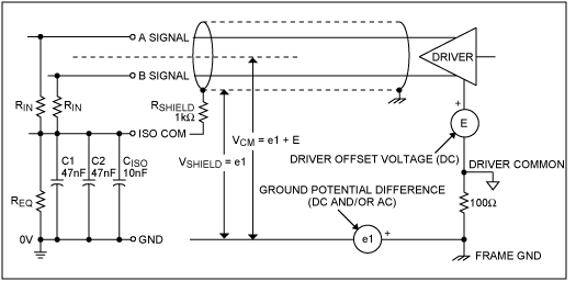
Figure 9. Equivalent input circuit for unshielded line.
The results of Equations 3 and 4 are presented graphically in Figures 10 and 11, and correspond well with laboratory measurements. Minor variations may be expected as experimental results were obtained from a single sample, and calculations were performed using typical values of RIN, and REQ, and nominal values for C1, C2, and CISO.
Note that, for AR and BR open, a 60Hz applied signal is limited to ≈ 25VPK for unshielded-cable connection, while even a 240Hz 47VPK signal may be applied in the case of the shielded-cable connection. In either case, when AR and BR are connected to ISO COM, the maximum frequency/voltage limitations are less severe. If 60Hz common-mode signals ≥ 25VPK are experienced on an unshielded-line connection, it may be necessary to make the AR, BR connection to ISO COM, even at the expense of forcing the MAX3157 to be a 1/6 U.L. receiver. The advantage of the shielded-line connection is apparent.
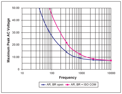
Figure 10. Maximum peak AC voltage vs. frequency applied at receiver inputs to produce ±7VPK across RIN for unshielded-cable connection.
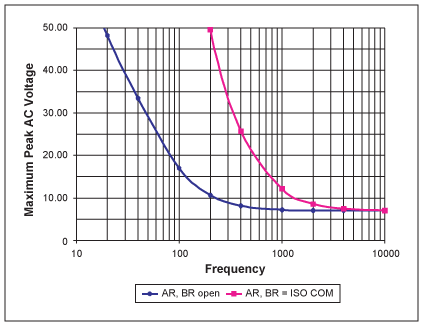
Figure 11. Maximum peak AC voltage vs. frequency applied at receiver inputs to produce ±7VPK across RIN for shielded cable connection with RSHIELD = 1kΩ.
Open-Line/Shorted-Line Fail SafeThe RS-485 specification defines receiver differential thresholds as +200mV and ?200mV. However, when a two-wire differential line is open circuited or when all drivers on the line are in their inactive states, the line signal voltage is undefined and could fall within the ±200mV receiver threshold limits. To ensure a defined receiver state when this condition exists, the RS-485 system guidelines suggest that a two-resistor network be placed at a single location on the two-wire line to pull one line toward +5V and the other line toward 0V to ensure a definite receiver state when all drivers are inactive. The resistor values, however, must be determined from a knowledge of the number of unit loads presented by the receiver circuit. This is suggested only where connected receivers do not include suitable open-line fail-safe circuitry. Most currently-available receivers4 do contain some sort of internal bias circuitry to provide a known output state when the inputs are open circuited, but these circuits may or may not provide complete fail-safe signaling for all possible conditions of line loading.
If the lines should become shorted together, zero- or near-zero voltage will be presented to the receiver's inputs to create an indefinite receiver-output state. To ensure a defined receiver state when this condition exists, the application guideline document suggests that a four-resistor network be placed on the line at each receiver input. This creates additional unit-loads on the line, and diminishes the maximum number of receivers that may exist on the line.
The MAX3157 creates fail-safe operation for either open or shorted lines by setting the receiver thresholds at -200mV and -50mV. This range falls within the RS-485 specification, and ensures a defined receiver logic-high output under all line-fault conditions whether shorted line, inactive-driver line, or open-circuited line.
Protection CircuitryThere are two back-to-back 50V-breakdown SCR devices in series inside the IC to protect the circuitry if the voltage between ISO COM and logic-ground should exceed approximately ±100V due to an ESD event. Specification limits for this voltage difference are ±75V due to potential inaccuracies in the SCR breakdown voltages. It is important that external resistance to cable ground be high enough to prevent establishing a holding current in these SCRs due to the ESD event. A resistor of not less than 1kΩ should be placed between ISO COM and the cable ground to satisfy this requirement.
There are internal SCR protection devices on each of the receiver inputs and transmitter outputs of the isolated side. The continuous current into A, B, Y, or Z must be limited to prevent latch-up after an ESD event. Continuous voltage on A, B, Y, or Z must be limited to -8 or +12.5V which exceed the RS-485 specification limits of -7V or +12V.
ConclusionBy utilizing a resistive-isolation technique and capacitive voltage transfer to power the isolated circuits, the MAX3157 functions as a low-cost replacement for capacitively-, optically-, or magnetically-isolated transceivers in the majority of systems requiring only moderate isolation-voltage capability. Additionally, it exhibits true fail-safe receiver performance. Its several other useful features are adequately described in the data sheet.
Notes
- TIA/EIA STANDARD TIA/EIA-485-A, Electrical Characteristics of Generators and Receivers for Use in Balanced Digital Multipoint Systems, Telecommunications Industry Association, March 3, 1998.
- TIA/EIA TELECOMMUNICATIONS SYSTEMS BULLETIN TSB89, Application Guidelines for TIA/EIA-485-A, Telecommunications Industry Association, June 1998.
- Throughout the remainder of this section, the labels A and B will be used to reference receiver inputs, although in RS-485 two-wire applications, the two-wire line is connected to terminals Y and Z.
- Maxim Application Note, Trim the Fat Off RS-485 Designs.
欢迎分享,转载请注明来源:内存溢出

 微信扫一扫
微信扫一扫
 支付宝扫一扫
评论列表(0条)