
基于STM8L15xxx设计的超低功耗8位MCU开发方案
ST公司的STM8L15xxx是超低功耗8位MCU系列,采用先进的STM8内核,动态功耗为192 μA/MHZ,16MHz CPU时钟的性能高达16 MIPS, 工作电压从1.8 V 到3.6 V (低至1.65 V ),多达32KB嵌入闪存程序存储器,主要用在医疗和手提设备,PC外设,游戏机,GPS,告警系统,有线和无线传感器.本文介绍了STM8L15xxx主要特性,方框图, 时钟树框图和超低功耗STM8L15LPBOARD演示板主要特性,详细电路图.
The STM8L15xxx devices are members of the STM8L Ultralow power 8-bit family. They are referred to as medium-density devices in the STM8L15xxx reference manual (RM0031) and in the STM8L Flash programming manual (PM0054). They provide the following benefits:
● Integrated system
– Up to 32 Kbytes of medium-density embedded Flash program memory
– 1 Kbyte of data EEPROM
– Internal high speed and low-power low speed RC.
– Embedded reset
● Ultralow power consumpTIon
– 192 μA/MHZ (dynamic consumpTIon)
– 1 μA in AcTIve-halt mode
– Clock gated system and opTImized power management
– Capability to execute from RAM for Low power wait mode and Low power run mode
● Advanced features
– Up to 16 MIPS at 16 MHz CPU clock frequency
– Direct memory access (DMA) for memory-to-memory or peripheral-to-memory access.
● Short development cycles
– Application scalability across a common family product architecture with compatible pinout, memory map and modular peripherals.
– Wide choice of development tools
The STM8L15xxx family operates from 1.8 V to 3.6 V (down to 1.65 V at power down) and is available in the -40 to +85℃ and -40 to +125℃ temperature ranges.
The STM8L15xxx Ultralow power family features the enhanced STM8 CPU core providing increased processing power (up to 16 MIPS at 16 MHz) while maintaining the advantages of a CISC architecture with improved code density, a 24-bit linear addressing space and an optimized architecture for low power operations.
The family includes an integrated debug module with a hardware interface (SWIM) which allows non-intrusive In-Application debugging and ultrafast Flash programming.All STM8L15xxx microcontrollers feature embedded data EEPROM and low power lowvoltage single-supply program Flash memory.
The modular design of the peripheral set allows the same peripherals to be found in different ST microcontroller families including 32-bit families. This makes any transition to a different family very easy, and simplified even more by the use of a common set of development tools.
These features make the STM8L15xxx microcontroller family suitable for a wide range of applications:
● Medical and handheld equipment
● Application control and user interface
● PC peripherals, gaming, GPS and sport equipment
● Alarm systems, wired and wireless sensors
STM8L15xxx 主要特性:
■ Operating conditions
– Operating power supply range 1.8 V to 3.6 V (down to 1.65 V at power down)
– Temperature range: - 40℃ to 85 or 125℃
■ Low power features
– 5 low power modes: Wait , Low power run (5.1 μA), Low power wait (3 μA), Active-halt with full RTC (1.3 μA), Halt (350 nA)
– Dynamic consumption: 195 μA/MHz+440μA
– Ultralow leakage per I/0: 50 nA
– Fast wakeup from Halt: 4.7 μs
■ Advanced STM8 core
– Harvard architecture and 3-stage pipeline
– Max freq. 16 MHz, 16 CISC MIPS peak
– Up to 40 external interrupt sources
■ Reset and supply management
– Low power, ultrasafe BOR reset with 5 selectable thresholds
– Ultralow power POR/PDR
– Programmable voltage detector (PVD)
■ Clock management
– 1 to 16 MHz crystal oscillator
– 32 kHz crystal oscillator
– Internal 16 MHz factory-trimmed RC
– Internal 38 kHz low consumption RC
– Clock security system
■ Low power RTC
– BCD calendar with alarm interrupt
– Auto-wakeup from Halt w/ periodic interrupt
■ LCD: up to 4x28 segments w/ step-up converter
■ Memories
– Up to 32 KB of Flash program memory and 1 Kbyte of data EEPROM with ECC, RWW
– Flexible write and read protection modes
– Up to 2 Kbytes of RAM
■ DMA
– 4 channels; supported peripherals: ADC,DAC, SPI, I2C, USART, timers
– 1 channel for memory-to-memory
■ 12-bit DAC with output buffer
■ 12-bit ADC up to 1 Msps/25 channels
– T. sensor and internal reference voltage
■ 2 Ultralow power comparators
– 1 with fixed threshold and 1 rail to rail
– Wakeup capability
■ Timers
– Two 16-bit timers with 2 channels (used as IC, OC, PWM), quadrature encoder
– One 16-bit advanced control timer with 3 channels, supporting motor control
– One 8-bit timer with 7-bit prescaler
– 2 watchdogs: 1 Window, 1 Independent
– Beeper timer with 1, 2 or 4 kHz frequencies
■ Communication interfaces
– Synchronous serial interface (SPI)
– Fast I2C 400 kHz SMBus and PMBus
– USART (ISO 7816 interface and IrDA)
■ Up to 41 I/Os, all mappable on interrupt vectors
■ Up to 16 capacitive sensing channels with free firmware
■ Development support
– Fast on-chip programming and non intrusive debugging with SWIM
– Bootloader using USART
■ 96-bit unique ID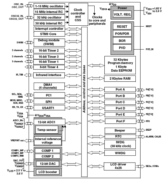
图1.STM8L15xxx方框图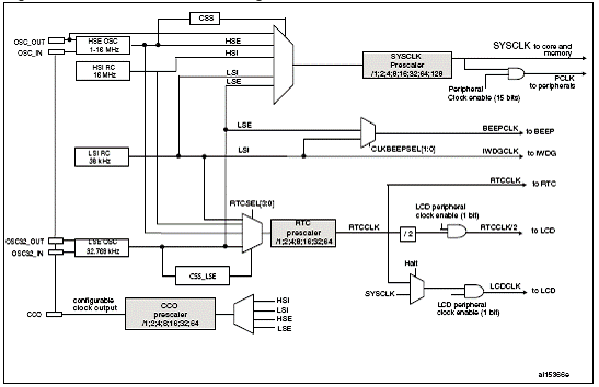
图2.STM8L15x时钟树框图
STM8L15LPBOARD超低功耗演示板
STM8L15LPBOARD low-power demonstration board The STM8L15LPBOARD low-power demonstration board demonstrates all the STM8L15x low-power modes, and permits the user to take consumption measurements in all modes.
STM8L15LPBOARD演示板主要特性:
■ SWIM debug support
■ MCU consumption auto-measurement circuit
■ Function and wakeup buttons
■ 32.768 kHz quartz
■ MCU pins connector
图3.STM8L15LPBOARD演示板外形图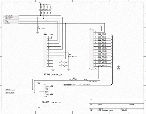
图4.STM8L15LPBOARD(MB870B)电路图(1)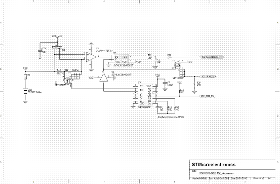
图5.STM8L15LPBOARD(MB870B)电路图(2)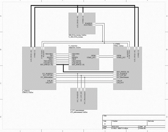
图6.STM8L15LPBOARD(MB870B)电路图(3)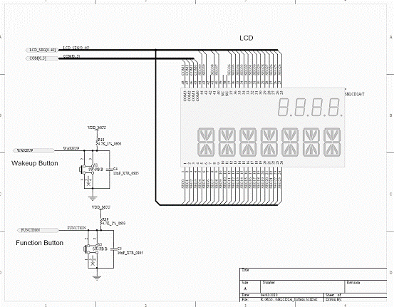
图7.STM8L15LPBOARD(MB870B)电路图(4)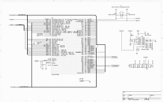
图8.STM8L15LPBOARD(MB870B)电路图(5)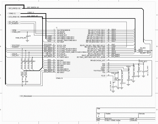
图9.STM8L15LPBOARD(MB870B)电路图(6)
欢迎分享,转载请注明来源:内存溢出

 微信扫一扫
微信扫一扫
 支付宝扫一扫
评论列表(0条)