副边变压器端接提升高速ADC的增益平坦度
Abstract: The following applicaTIon note describes the differences between primary- and secondary-side terminaTIon of a transformer commonly used in signal condiTIoning circuits preceding high-speed analog-to-digital converters (ADCs). It details the impacts of these two terminaTIon schemes on the gain flatness and the dynamic performance of an ADC designed for high-IF applications.
The proper selection of input network components is crucial to the drive and balance of the input network of high-speed analog-to-digital converters (ADCs) (See the application note: "Proper Input Network Selection Achieves Optimum Dynamic Performance and Excellent Gain Flatness in High-Speed ADC.")
In high-IF applications, the location of the termination impedance becomes particularly important. Depending on the requirements for gain flatness and dynamic performance, an AC-coupled input signal can be terminated on either side of the transformer. Wide-band transformers are popular components that support a fast and easy way to convert a single-ended signal to a differential signal over a wide range of frequencies.
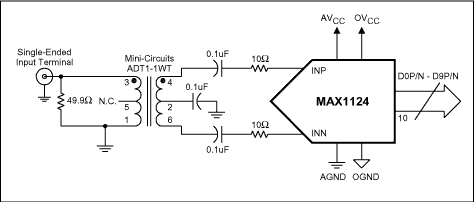
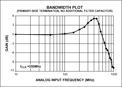
For this application note, the MAX1124 - Maxim's recently introduced 250MHz, 10-bit high-IF ADCs - was selected to demonstrate different termination schemes and their impact on gain bandwidth and dynamic performance of the ADC. Starting with a primary-side termination configuration (Figure 1a), a 50Ω -impedance source signal was applied to the ADT1-1WT transformer's primary side. Its secondary side connected directly to the input filter network (10Ω isolation resistor + input impedance of the ADC) of the MAX1124 through 0.1µF AC-coupling capacitors. No additional input filter capacitors were installed on INP and INN. In this configuration, the primary side of the transformer is well balanced, however the secondary side looks straight into the nominal 4kΩ /3pF input impedance of the ADC. The imbalance on the secondary side, combined with the leakage inductance of the transformer generates a resonant circuit, which produces maximum frequency peaking between 450MHz and 550MHz (Figure 1b). 
Figure 1a.
Figure 1b.
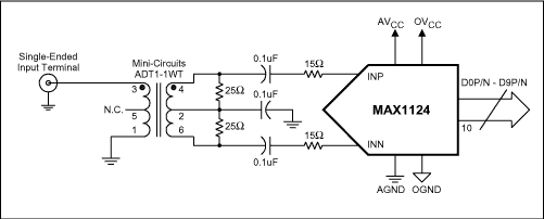
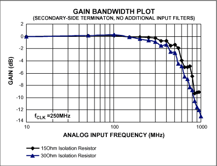
To eliminate frequency peaking almost completely while driving the input differentially, the primary-side termination was removed and the 50Ω -source impedance signal was applied to the ADT1-1WT with secondary-side termination instead. Secondary-side termination in this case means two 25Ω resistors placed between top/bottom and center tap of the transformer (Figure 2a). Followed by 0.1µF capacitors for AC-coupling purposes and an input filter network (15Ω series resistor + the input impedance of the ADC), a well-balanced secondary-side signal is now applied to the converter. As with the configuration Figure 1, no additional input filter capacitors are installed on INP and INN. With this configuration, frequency peaking in the range of 450MHz to 550MHz can be completely eliminated. If required, more DC attenuation can be added by exchanging the 15Ω isolation resistors for 30Ω resistors. Although this approach makes the frequency response smoother, it comes at the cost of loss in frequency bandwidth (Figure 2b).
Figure 2a.
Figure 2b.
This application note has shown that not only does the proper choice of passive components play an important role in designing input networks for high-speed data converters, the proper use of these components is significant as well. For instance, if gain flatness is an important factor in a system, care must be taken to avoid imbalances and resonances at the differential inputs of the converter to ensure that its true dynamic performance can be replicated.
Also, the fact that both configurations do not use filter capacitors at their inputs may raise some concern about the impact of additional noise pick-up at INP and INN. This was briefly analyzed as well and resulted in a degradation of the signal-to-noise ratio (SNR) between 0.2dB to 0.5dB. As long as wide bandwidth and stability over a wide range of frequencies (short: gain flatness) and a high dynamic performance is desired, most high IF applications will likely accept this rather minor degradation in noise performance for a 10-bit data converter.
MAX1122 pdf,MAX1122 datasheet
欢迎分享,转载请注明来源:内存溢出

 微信扫一扫
微信扫一扫
 支付宝扫一扫
评论列表(0条)