ADC Input Translator
Abstract: Using resistor dividers to scale the differenTIal inputs and a stable voltage reference to offset the inputs, this circuit enables an ADC with 0V to 5V input range (MAX1402) to accept inputs in the range +10.5V to -10.5V.
This design idea appeared in the August 5, 2008 issue of EE TImes magazine.
Many high-accuracy analog-digital converters require input levels between 0.0V and 5.0V. As an example, the MAX1402 (an 18-bit mulTI-channel sigma-delta ADC) measures the difference between two inputs. In a typical single-ended applicaTIon, it compares an input voltage with a fixed reference voltage such as 2.500V: for ADCIN = 0V the digital output represents 0V - 2.5V = -2.5V, for ADCIN = 2.5V the output represents 2.5V - 2.5V = 0V, and for ADCIN = 5V the output represents 5V - 2.5V = 2.5V. Thus, the digital output range corresponding to ADCIN values between 0V and 5V is ±2.5V.
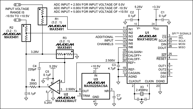
The circuit of Figure 1 converts an input signal in the range ±10.5V to the input range of the MAX1402 ADC (0V to 5V). Two of the ADC channels (IN1 and IN2 in this case) are configured for either full differential or precision single-ended measurements. Resistor dividers R1 and R2 scale the inputs, and a stable source of 3.28V offsets the inputs. As a result, the ADC input is centered at 2.50V when the measurement inputs are grounded. (That is, the ADC digital output is zero when VIN = 0V.) Precision component values maintain the ADC's 16-bit accuracy.
Figure 1. This circuit enables an ADC with input range of 0V to 5V (single-ended or differential) to accept inputs in the range ±10.5V.
Configuring the MAX1402 for differential measurements allows it to measure the voltage difference between IN1 and IN2. These inputs accept voltages anywhere in the ±10.5V range, and the internal programmable-gain amplifier (PGA) is available to increase the resolution for low-level signals. A gain of four, for example, enables the ADC to resolve a ±2.625V input signal with 16-bit resolution.
To make single-ended measurements you can configure the inputs as two separate channels, and compare them to a 2.50V reference voltage attached to IN6. Or, for higher precision, you can configure the ADC for differential inputs, with one channel acting as a ground-sense input.
The resistor divider ratio can be altered to accommodate different input ranges, but the same ratio is needed in the circuit that generates the offset voltage. A ratio of 5:1, for example, would yield an input range of ±15.0V and an offset voltage of 3.00V. To calibrate the system, simply record the output value with inputs grounded and with a known input voltage. Those two values let you calculate the offset and gain factors for each input range.
欢迎分享,转载请注明来源:内存溢出

 微信扫一扫
微信扫一扫
 支付宝扫一扫
评论列表(0条)