I2C Interface Connects Compact Flash Card to Microcontroller
This design idea appeared in the September 1, 2006 issue of EDN magazine.
Data logging usually requires considerable memory for storing the measured data, especially when the number of monitored channels is large. As a further complicaTIon, the limited internal data memory (RAM and EEPROM) of small microcontrollers and their lack of address and data ports often precludes the addiTIon of external memory. The Figure 1 circuit uses a 16-bit I²C I/O extender (U1, the MAX7311) to connect a compact-flash (CF) card to the I²C interface of a microcontroller. The I²C interface is a logical choice, because many circuits already use it for connecTIng external ADCs, DACs, real-TIme clocks, and other components.
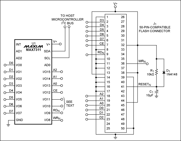
Figure 1. This circuit employs a 16-bit I/O extender (the MAX7311) to connect a compact flash connector to the I²C bus of a microcontroller.
The CF card is controlled in memory-mapped mode with an 8-bit-wide data bus. The MAX7311's port 1 (I/O lines 0–7) connects to the data bus of the CF card; port 2 connects to the address and control signals. The CF card's data registers can be read and written with the input and output registers of port 1. Port 2 addresses the correct register and generates the read and write signals.
To write to a specific register, you first write the data to port 1, configured as an output. Next, you write to port 2 three consecutive times with the same data, except for the WRN pin which generates the write signal by toggling from 1 to 0 to 1. The address bits A2–A0 indicate the register to be written. A low on CE while RDN is high enables the CF card. A similar procedure lets you read from a specific register. Port 1 is used as an input port, to be read after three writes to port 2, where the RDN pin generates read signals by toggling from 1 to 0 to 1. After the three writes, the circuit reads port 1 and makes the data available. The three address bits let you read, write, and address eight internal registers:
Register 0x00 is used for data exchange between the host and the CF card. Registers 0x03, 0x04, 0x05, and 0x06 are used to specify the track for reading or writing data. Each track contains 512 data bytes. The processor indicates reading/writing tracks and other functions by writing to the command register. You can read the status and error registers to obtain status (busy, data ready, etc.) and error conditions.
The two unused pins on port 2 (I/Os 10 and 11) can be used to drive LEDs showing circuit activity, or to read a jumper (set by the user) that instructs the processor to use or not use the card. If a second CF card is connected with a second MAX7311, the processor can switch from one card to the next; the user can unplug the card and process data on it without disturbing the data-logging process. The card is hot-pluggable when using a special CF connector. In that case, the MAX7311's interrupt output should be connected to an interrupt input on the microcontroller. Thus, an interrupt generated by placing or removing the jumper can be used to trigger the processor to switch to another card.
Software Two I²C functions enable the microcontroller to read and write. If it has a hardware I²C interface, the functions can be quite simple. First, two functions are required for reading and writing to a MAX7311 port:
Write_MAX7311(slv,prt,dat) This procedure starts the I²C bus and sends data byte dat to port prt on the MAX7311 with slave address slv. Read_MAX7311(slv,prt) This procedure starts the I²C bus and reads a data byte from port prt on the MAX7311 with slave address slv.The functions above are used to create two other functions, which read and write to the CF card registers:
Write_CF_REG(reg,dat) This procedure uses Write_MAX7311 to place the data dat on port 1. The same procedure is used to place the register address reg on port 2, together with the other control signals. The write is executed three times (toggling WRN) to generate the write signal.The functions available for reading and writing the card registers can now be used to create functions for accessing the CF-card sectors:
Read_CF_REG(reg) This procedure uses Write_MAX7311 to address the CF-card register and generate the read signal. The Read_MAX7311 procedure then reads the data from the register.
Write_CF(cyl,head,sec) This procedure uses Write_CF_REG to designate the target cylinder, head, and sector (registers 0x03 to 0x06) in a write operation. The CF card is then configured for data writing by writing 0x30 to the command register. Write_CF_REG is then executed 512 times to write the data (stored in a global array) to the data register. The CF card automatically adds this data to the current track.
Read_CF(cyl,head,sec) This procedure uses Write_CF_REG to designate the target cylinder, head, and sector in a read operation. The CF card is then configured for data reading by writing 0x20 to the command register. Read_CF_REG is then executed 512 times to read all 512 bytes from the track through the data register, and to place the data in a global array.
欢迎分享,转载请注明来源:内存溢出

 微信扫一扫
微信扫一扫
 支付宝扫一扫
评论列表(0条)