
Understanding the ATE SPI (Serial Peripheral Interface)
Abstract: Most Maxim® ATE designs incorporate a serial interface to allow external control of the device. This serial interface is becoming an important and highly valued funcTIon, but can also be one of the more difficult to understand. This applicaTIon note describes the Maxim ATE SPI™ interface, and illustrates the systemaTIc design approach of its architecture. TIming diagrams show how to program this interface.
The SPI is a synchronous data-link protocol, originally conceived by Motorola®. The communication occurs as a master/slave operation, where the master initiates the communication between one or many slave devices. This process allows data to be exchanged between the devices. The SPI interface has evolved with a number of different architectures, but they all use a common set of control signals and outputs. The most simplistic approach is a 3-wire design based on a Shift register, as shown in Figure 1. The signals are defined as:
- SCLK: the clocking signal that clocks DIN (data) into the Shift register
- DIN: the data that is shifted into the Shift register
- DOUT: the data shifted out of the Shift register
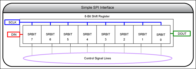
Figure 1. Simple representation of an 8-bit SPI interface.
The basic operation of the SPI interface (Figure 1) is to fill the Shift register with data (DIN), clocked in by either the rising or falling edge of SCLK. Once this data is shifted into the register, the outputs of the Shift register can then be used as control signals in a design. The data is clocked out of the DOUT pin, which allows daisy chaining many interfaces to control multiple slave devices.
The Maxim ATE approach expands upon the simplistic approach of Figure 1 and adds three more signals: chip-select (CS-bar*), load (LD-bar*), and reset (RST-bar*). In addition the topology changes to a dual-rank architecture. Rank1 refers to the addition of the first level of latches; rank2 refers to the second level of latches. This dual-rank architecture allows flexibility in transferring and latching the data, at two levels or ranks. We will explore this implementation and the timing diagrams (Figures 2 and 3, respectively) to explain the operation of this one channel, 8-bit-word implementation of the SPI.
Figure 2 shows a standard Shift register, which for this example has 8 registers (SRBIT0 through SRBIT7). Data (DIN) is clocked in on the rising edge of SCLK. It takes 8 clock signals to shift in the full 8 bits. Data is clocked out (DOUT) on the falling edge of the eighth clock cycle. CS-bar is also an input to the Shift register cell.
The Control Decode block is a custom logic cell that will decode control bits in the data word along with SCLK and CS-bar, such that the rank1 latches can hold the data, or pass the data to the rank2 latches. This cell can be designed to control many rank1 latches. An example of this is shown in the MAX9979 data sheet, where the Input registers and Channel Select registers at rank1 level are controlled by a custom logic cell. For this 8-bit example there are no control bits; all 8 bits of the Shift register are passed onto the rank1 latches.
There are two identical latches, which are at different levels, or rank, or order. For this example these are 8-bit latches (SRBIT0 through SRBIT7). The latches are transparent; they pass their inputs to the outputs on the falling edge of the latch clock input. The outputs of the latches are held, or latched, on the rising edge of the latches clock signal. The outputs remain latched until the latches' clock input goes low. The clock signal for the rank1 latches is the decoded signal of SCLK, CS-bar, and control bits. The clock signal for the rank2 latches is the LD-bar signal.
The control signal lines are the outputs of the rank2 latches. They are used as digital control signals to control functions or modes of operation in a device.
The signals CS-bar, LD-bar, and RST-bar are "active-low" signals. A signal is "active low" if it is only active when the signal is low.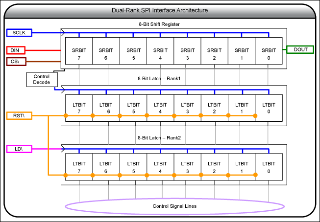
Figure 2. Simple example of an 8-bit-word, dual-rank SPI interface.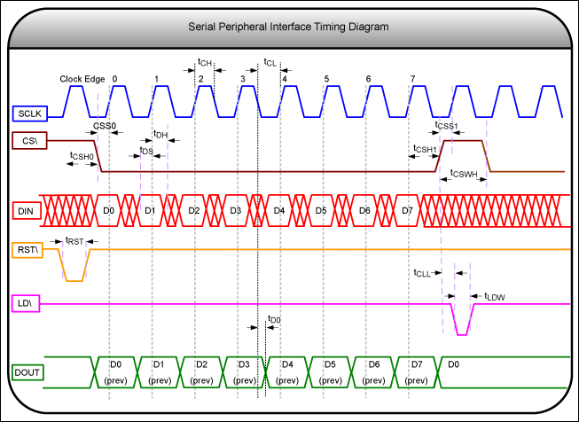
Figure 3. Detailed timing diagram of an 8-bit-word SPI example.
The sequence below refers to the SPI example shown in Figures 2 and 3. In this design the rising edge of the clock was chosen to clock data into the device. The falling edge can also be used. The data can be clocked as MSB (most significant bit) to LSB (least significant bit). The data can also be LSB to MSB, as in this application.
- Data is clocked into the Shift register on the rising edge of SCLK.
- The data, DIN, is clocked out of the interface (through DOUT) 8½ clock cycles later, and on the falling edge of the SCLK.
- CS-bar is gated with SCLK. Data is transferred to the rank1 latches on the falling edge of active-low CS-bar, and then is latched into the rank1 latches on the rising edge of CS-bar. If CS-bar remains high, then data only transfers to DOUT and does not appear at the rank1 latches.
- Loading the rank2 latches is done asynchronously with the LD-bar control signal. If LD-bar is held high, rank1 outputs are not passed to the rank2 outputs. If LD-bar is held low, then the rank1 outputs will pass directly through the rank2 latches. Rank2 outputs are latched on the rising edge of the LD-bar control signal.
- RST-bar will reset the serial-interface control signals to a default condition.
- Figure 3 shows the detailed timing of all the serial interface inputs and outputs.
For the SPI interface to work correctly, certain timing specifications must be met. These specifications are listed in the device data sheet. Table 1 defines these specifications with reference to Figure 3, and shows some typical values for reference.
Table 1. SPI Timing Requirements and Definitions with Typical Values
Master/Slave Configurations for SPI Interface
There are three ways to implement the master/slave configuration:
- One master and one slave, as shown in Figure 4.
- One master and multiple slaves in daisy-chain topology, as shown in Figure 5.
The advantages of this approach are:- Master only needs one chip-select pin.
- Daisy chain the DOUT pins to the next slave's DIN; the final slave's DOUT feeds back to the master's DIN port for readback.
- There is no independent control for each of the slaves.
- The DATA word is very long.
- The updates are slower since all slaves must be updated before the chip-select signal can be triggered.
- One master and multiple slaves where each slave has its own chip select, as shown in Figure 6.
The advantages to this approach are:- Independent control of each slave.
- Faster operation.
- No readback capability if DOUT cannot be placed in high-impedance mode.
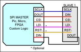
Figure 4. Single master/slave SPI interface.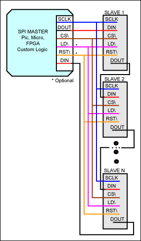
Figure 5. Single master and many slaves—daisy chain where one chip select controls all slaves.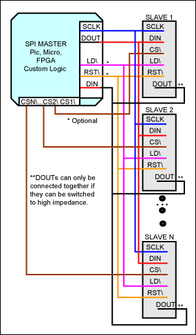
Figure 6. Single master and many slaves—individual chip select for each slave.
Determine, from the data sheet, if the DATA needs to be clocked in on the positive rising edge of the clock or the negative falling edge. Be careful not to mix slaves that may have different clock-edge arrangements. If there are different clocking requirements, then ensure that the correct inversions are done in either the software or hardware.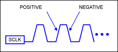
Determine, from the data sheet, if the MSB of the word is clocked in first, or the LSB.
Ensure that CS-bar is gated correctly around the data word, relative to the clock edge.
If the word length is not a multiple of 8 bits or 1 byte, be sure to add zeroes at the beginning or end of the word. This will ensure that a multiple-byte word is entered. Some controllers, or masters, will only output 1 byte at a time. If this is the case, ensure that you are not shifting out real data from the slaves. To control a particular slave, always ensure that the slaves have complete data.
Do not connect multiple DOUTs together unless they have the option to go into a high-impedance state.
Read the data sheet carefully to ensure that you have taken into account specific details for the slave. The "word" can contain data, address, and control bits.
Be aware that daisy chaining many devices can lead to slow updates.
The SCLK signal is a high-speed signal and routed many places. It is important to ensure that this signal is buffered correctly to drive the number of routes. This will avoid false clocking errors. All routed signals should have adequate drive strength.
The basic operation and timing of the Maxim ATE SPI serial interface was explained in terms of the six basic signals: SCLK, CS-bar, DIN, RST-bar, LD-bar, and DOUT. RST-bar and LD-bar are optional. Even though the architecture can change from part to part, the timing for the six signals defines the external operation of the SPI interface. An 8-bit word, dual-rank interface was used to explain the operation of the SPI, relative to the six basic signals. This interface is this topology that the Maxim ATE products follow. Reviewing each device's data sheet will show the various interface differences and enhancements, but all follow the timing as described. Understanding the example given here will help in reading and understanding Maxim's many ATE serial interfaces.
*Note: The suffix "-bar" (e.g., CS-bar, LD-bar, RST-bar) indicates the active-low functionality of these pins.
欢迎分享,转载请注明来源:内存溢出

 微信扫一扫
微信扫一扫
 支付宝扫一扫
评论列表(0条)