
The ADS58C48 is a quad channel 11-bit A/D converter with sampling rate up to 200 MSPS. It uses innovaTIve design techniques to achieve high dynamic performance, while consuming extremely low power at 1.8V supply. This makes it well-suited for mulTI-carrier, wide band-width communicaTIons applications.
The ADS58C48 uses third-generation SNRBoost3G technology to overcome SNR limitation due to quantization noise (for bandwidths < Nyquist, Fs/2). Enhancements in the SNRBoost3G technology allow support for SNR improvements over wide bandwidths (up to 60 MHz). In addition, separate SNRBoost3G coefficients can be programmed for each channel.
The device has digital gain function that can be used to improve SFDR performance at lower full-scale input ranges.
ADS58C48主要特性:
Maximum Sample Rate: 200 MSPS
High Dynamic Performance
SFDR 82 dBc at 140 MHz
72.3 dBFS SNR in 60 MHz BW Using SNRBoost3G technology
SNRBoost3G Highlights
Supports Wide Bandwidth up to 60 MHz
Programmable Bandwidths – 60 MHz, 40 MHz, 30 MHz, 20 MHz
Flat Noise Floor within the Band
Independent SNRBoost3G Coefficients for Every Channel
Output Interface
Double Data Rate (DDR) LVDS with Programmable Swing and Strength
Standard Swing: 350mV
Low Swing: 200mV
Default Strength: 100
 Termination
 2x Strength: 50
 Termination
1.8V Parallel CMOS Interface Also Supported
Ultra-Low Power with Single 1.8V Supply
0.9W Total Power
1.32 W Total Power (200 MSPS) with SNRBoost3G on all 4 Channels
1.12 W Total Power (200 MSPS) with SNRBoost3G on 2 Channels
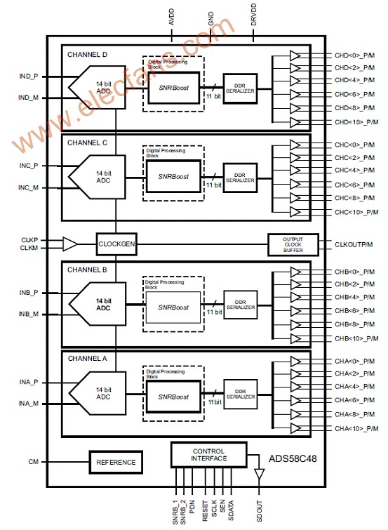
图1。ADS58C48方框图(LVDS接口)
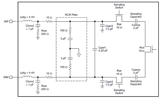
图2。ADS58C48模拟输入电路图

图3。ADS58C48低带宽驱动电路(低输入频率)

图4。ADS58C48高带宽驱动电路(高输入频率)
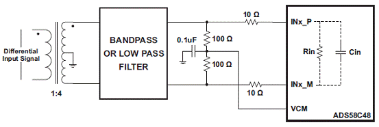
图5。ADS58C481:4变压器驱动电路)
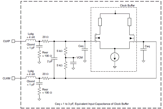
图6。ADS58C48内部时钟缓冲器电路
ADS58C48EVM评估板
The ADS58C48EVM is a circuit board that allows designers to evaluate the performance of Texas Instruments’ ADS58C17 device, a low power, four channel 11-bit 200 MSPS analog to digital converter featuring TI’s SNRBoost technology. The ADC EVM features a DDR LVDS data output which is compatible with TI’s TSW1200 data capture card for rapid evaluation. The EVM provides a flexible environment to test the ADS58C48 under a variety of clock, input and supply conditions.
图7。ADS58C48EVM评估板外形图
The evaluation module is designed with bakc-to-back wide bandwidth baluns on each of the converter’s four inputs. This enables a wide sweep of single-ended input signals to be input into any channel of the ADC.
The ADS58C48EVM is also compatible with the FMC-ADC-Adapter and the HSMC-ADC-Bridge EVMs. The adapater and bridge cards enable the ADS58C48 to mate with FMC and HSMC connectors found on Xilinx and Altera FPGA development kits, respectively. This enables rapid system level software prototyping without having to develop a custom prototyping board.
ADS58C48EVM评估板主要特性:
USB input for SNRBoost and other SPI register controls
Transformer coupled analog input path
Transformer coupled clock input path
Direct connection to TSW1200EVM High Speed ADC Data Capture Card
Compatible with FMC-ADC-ADAPTER and HSMC-ADC-BRIDGE for direct connection to FPGA development kits
Separate analog and digital supply connections or single 5V global supply
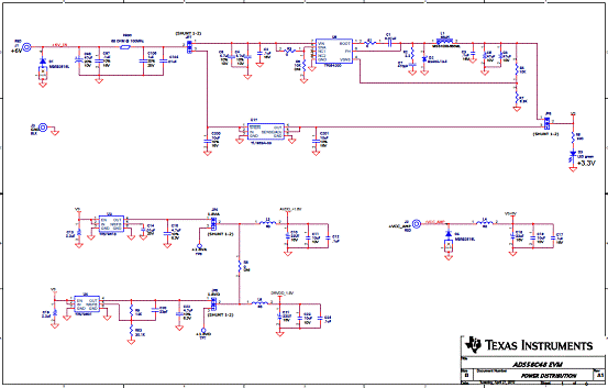
图8。ADS58C48EVM评估板电路图(1)
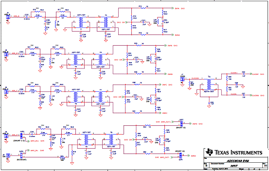
图9。ADS58C48EVM评估板电路图(2)
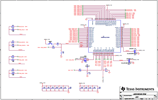
图10。ADS58C48EVM评估板电路图(3)
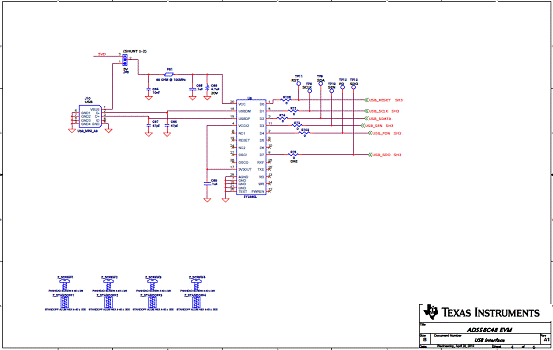
图11。ADS58C48EVM评估板电路图(4)
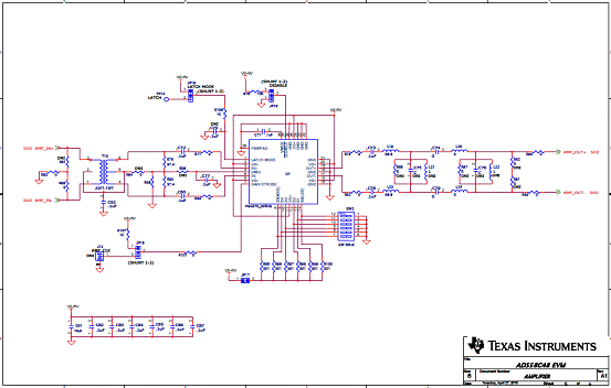
图12。ADS58C48EVM评估板电路图(5)
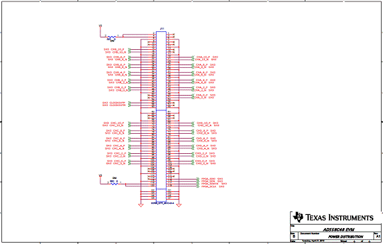
图13。ADS58C48EVM评估板电路图(6)
欢迎分享,转载请注明来源:内存溢出

 微信扫一扫
微信扫一扫
 支付宝扫一扫
评论列表(0条)