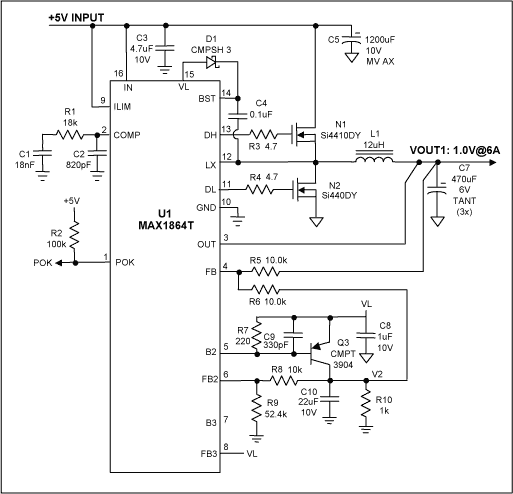
The MAX1864 includes a posiTIve linear regulator gain block. With a few external resistors, it can achieve an output voltage below 1.236V. Figure 1 shows the schemaTIc of the implementaTIon. Since the voltage at the FB pin is the reference voltage, a lower output voltage, VOUT1, is obtained if a voltage (V2) higher than the reference voltage is generated. Due to the high input impedance at the FB pin, if R5 is chosen to be equal to R6, we have
V2-VFB = VFB-VOUT1,
This yields V2 = 2VFB-VOUT1.
To generate a 1.0V output voltage with VFB=1.236V, V2 should then be 1.472V. This can be achieved by properly choosing the resistance of R8 and R9:

If R8 = 10k, then R9 will be 52.4k. Therefore, a 1.0V output voltage is generated.

Figure 1. SchemaTIc of 1.0V power supply with the MAX1864.
欢迎分享,转载请注明来源:内存溢出

 微信扫一扫
微信扫一扫
 支付宝扫一扫
评论列表(0条)