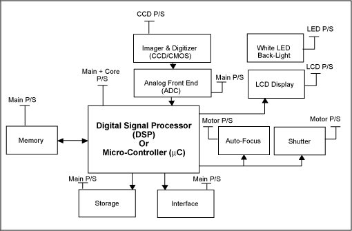

Figure 1. Block diagram of a typical digital still camera.
Most of the DSC systems also have a sub-processor (not shown in Figure 1), which contains a real-time clock and memory controller. The sub-processor is powered by an always-on back-up supply to keep the sub-processor blocks alive during system shutdown. Some manufacturers prefer that this supply be separated from the main battery supply to save battery life. In such systems an additional converter is necessary to provide the always-on backup power supply to the sub-processor.
The MAX1802 provides a complete single chip solution for powering the major blocks in digital still cameras and video cameras by integrating a high-efficiency step-down controller and converter each, and three auxiliary step-up controllers. The step-down controller is typically used for the main system power supply and the converter as the core power supply. The three auxiliary controllers are used for the LCD, CCD and motor power supplies. The MAX1801 is a slave controller that can be used with the MAX1802 to generate an independent LED power supply, if necessary. The MAX1802 operates in a low-noise constant frequency PWM mode and the MAX1801 is synchronized to the MAX1802 oscillator.
The MAX1802 IC was targeted for applications that use three or four alkaline cells, or two Li+ cells, as the basic power source to the system. However, some camera manufacturers are making a transition from 4AA cells to 2AA cells or 2 NiMH. In systems with only 2AA batteries, but using a back-up power supply, the MAX1802 can be used in conjunction with a high-efficiency step-up MAX1833 converter. The MAX1833 serves as a back-up power supply and the MAX1802 provides the supply for all the DSC system blocks.
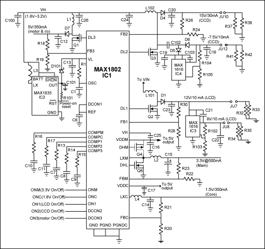
The application circuit for such a system is shown in Figure 2, indicating the various blocks in the camera system to be powered by the MAX1802. The approach makes it possible to implement the configuration with minimal increase in component count. In addition to providing back-up power to the sub-processor, the MAX1833 helps to power the MAX1802 at start-up.

Figure 2. The MAX1802 application circuit for DSC (2AA cells as input).
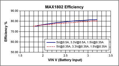
The MAX1802 uses an internal linear regulator powered from its VDDM pin to power the internal circuitry. The output of this linear regulator is seen at VL. The MAX1802 has an under-voltage lockout threshold of 2.4V at the VL pin. At power-up the VL pin of the MAX1802 is forced to a diode drop below 3.3V using the MAX1833 (Figure 2). The internal parasitic body diode of the LDO pulls up VDDM. This allows the internal reference and oscillator circuits for the MAX1802 to start-up. This in turn enables the auxiliary controller designed for a 5V output that is also used to run the motor. The 5V output is used to power up the 3.3V output step-down controller through VDDM (used as main system supply) and 1.5V output step-down converter (used for core processor power) through VDDC (Figure 2). The efficiency for this circuit at different loads and input voltages is shown in Figure 3.

Figure 3. Efficiency curve for the MAX1802 with 2AA cell input.
This data indicates that the MAX1802 is an efficient solution for a portable system power supply where component count and board real estate are critical issues even when the input voltage is lower than the range specified in the MAX1802 data sheet.
欢迎分享,转载请注明来源:内存溢出

 微信扫一扫
微信扫一扫
 支付宝扫一扫
评论列表(0条)