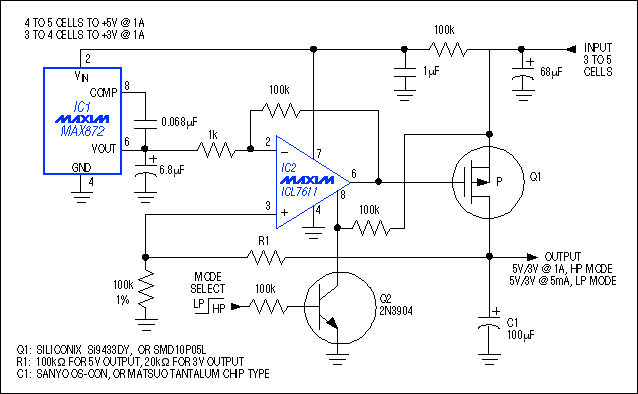

Figure 1. A p-channel MOSFET (Q1) allows this linear regulator to operate with VIN to VOUT differenTIals lower than 100mV.
This capability lets the Figure 2 circuit derive 5V ±10% from four battery cells, even when they've discharged as low as 4.6V. Low dropout voltage lets the circuit "ride down" on the declining battery voltage, finally falling out of regulaTIon at approximately 4.6V. The low input-to-output differential at that time (0.1V) allows nearly 100% efficiency. Note that the output accuracy of IC1 (±0.6% over temperature) makes it suitable as a 2.5V system reference.

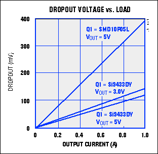
Figure 2. At low output current, these p-channel MOSFETs exhibit low source-to-drain voltage (i.e., dropout voltage in the Figure 1 circuit).
IC2's pin-programmable bias current makes possible a low-power mode in which the entire circuit draws less than 50µA. Five milliamps is available in this mode for circuitry such as backup RAM and a real-time clock. In high-power mode, the regulator can deliver 1A.
The 100µF output capacitor (C1) is chosen to accomodate the maximum load currents of 1A; for lighter loads you can scale the capacitor to a smaller value. Beware, though-the circuit's loop stability depends on lag compensation in which 1/2πRESRC1 > 14kHz, where RESR is C1's equivalent series resistance. (Figure 1 recommends acceptable capacitor types for C1.)
Configured for a 5V output (R1 = 100kΩ), the circuit can deliver 500mA from five cells producing 7.5V, or 1A from four cells producing 6V. Configured for 3V (R1 = 20kΩ), it delivers 500mA from four cells producing 6V, or 1A from three cells producing 4.5V. The input voltage can range from 3V to 15V, subject to a limitation; with no heatsink on Q1, the MOSFET's package-dissipation rating limits the input voltage and output current as follows: IOUT × (VIN - VOUT) < 1.25W.
欢迎分享,转载请注明来源:内存溢出

 微信扫一扫
微信扫一扫
 支付宝扫一扫
评论列表(0条)