Early digital-to-analog converters (DACs) were designed with standard R-2R ladders, and produced a negaTIve output voltage. These early DACs (such as the MX7837/MX7847 and MAX523) require both a posiTIve and a negative supply rail to accommodate their negative output. With the transition to single-supply integrated circuits, however, many modern DACs now operate with a single supply rail and an inverted R-2R ladder. The inverted R-2R ladder produces a positive output voltage.
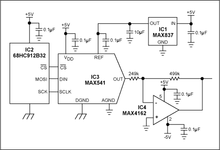
Despite the popularity of single-supply ICs, some applications still require a negative control voltage. One solution for this purpose is a modern, inverted R-2R ladder DAC and op amp (Figure 1). When compared with older DACs containing standard R-2R ladders, this approach offers lower supply voltages, higher speed, and smaller packages.

Figure 1. This compact circuit enables microcontroller IC2 to generate a variable negative voltage.
The DAC (IC3), operating with a 2.5V applied reference voltage from IC1 and driven by microcontroller IC2, produces an output swing from 0V to 2.5V. Op amp IC4 inverts and amplifies this output to produce a 0V to -5V output. For test purposes, a software routine enables the microcontroller to generate a 0V to -5V triangle-wave output.
Please note that the output impedance of the DAC (IC3) is 6.25kΩ ±20%. To eliminate system gain errors that are caused by the DAC's output impedance, buffer the DAC output before the IC4 inverting stage.
A similar version of this article appeared in the December 6, 2001 issue of EDN magazine.
欢迎分享,转载请注明来源:内存溢出

 微信扫一扫
微信扫一扫
 支付宝扫一扫
评论列表(0条)