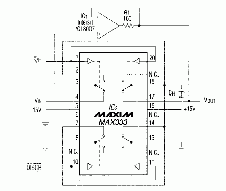

Figure 1. This Quad analog switch and general-purpose op amp from a low-cost sample/hold suitable for moderate-speed aplicaTIons.
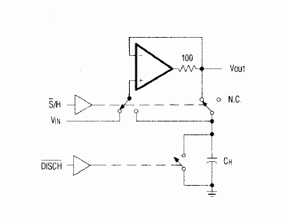
The two digital inputs are compaTIble with TTL and CMOS logic levels. Input command acTIve-low S/H controls the operating mode (low is sample), and DISCH is an optional control input whose low state commands a rapid and complete discharge of CH. Figure 2 provides a simplified functional diagram of the circuit.

Figure 2. A simplified version of Figure 1 illustrates how the analog switches shift the op amp from the role of input buffer to that of an output hold-capacitor buffer.
A general-purpose op amp is suitable for IC1, provided the input bias current is acceptable (bias current usually dominates the hold-mode droop rate). CH can range from 100pF to 0.1µF. In driving such a capacitive load, most op amps will oscillate without an isolating resistor (R1) of 100 to 200Ω within the feedback loop. Using components as shown in Figure 1, the typical circuit performance includes: droop rate ≤ 100mV/sec, aperture time ≤ 100nsec, offset voltage ≤ 5mV, output charge injection ≤ 25pC, an acquisition time ≤ 1µsec (for ±10% accuracy) or ≤ 5µsec (for ±0.1% accuracy)
Performance is about the same for ±15V or ±12V supplies, and the system also work well on a unipolar supply of 10 to 30V. Whatever the supply configuration, the op amp's common-mode range restricts VIN to about 2V less than the supply rails. The control inputs' TTL/CMOS switching thresholds (0.8V max, 2.4V min) remain constant regardless of supply levels
欢迎分享,转载请注明来源:内存溢出

 微信扫一扫
微信扫一扫
 支付宝扫一扫
评论列表(0条)