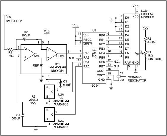
The simple 3V analog-to-digital converter (ADC) shown in Figure 1 is very small, requires no negaTIve supply or expensive precision components, and draws minimal supply current (10µA). A single conversion consists of 12,000 comparisons and takes about 300ms. The circuit operates as described below.

Figure 1. This inexpensive, 0.05%-linear ADC can be added to exisTIng equipment or used to upgrade the converter included in certain µCs (such as the PIC 16C71).
Following each comparison, the microcontroller (µC) closes one of two switches: IC2A (comparator high) or IC2B (comparator low). The switches connect either VREF (1.2V) or ground to their "B" terminals, producing a pulse-width modulaTIon (PWM) signal that is filtered by R3 and C1 and differentially integrated against VIN. The result is compared against VREF.
As this action integrates the error voltage up and down, the µC counts the number of comparisons for which the comparator output is high (IC2A switch closed). This count (NH) divided by 12,000 equals the PWM duty cycle. The system is fully ratiometric, so the duty cycle equals NH/12000 = VIN/VREF. Rearranging and substituting VREF = 1.2V yields VIN = NH/10,000.
Listing 1* enables the the LCD module to display voltage values directly, like a digital panel meter. The subroutine "DVM" produces the actual A/D-conversion values required in an embedded application. Setting the span constant (number of comparisons) to 12,000 yields a 300ms conversion with 4-1/2 digits of resolution and produces a 1.1999 full-scale display. You can speed the conversion to 30ms by setting the span constant to 1200, which produces a 3-1/2 digit display that reads 1.199 at full scale.
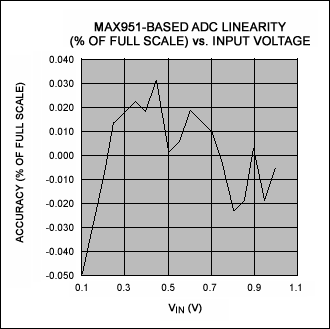
IC2's near-ideal switching characteristics account for the low 0.05% nonlinearity. A high-performance, 3V-specified version of the industry standard 4066, IC2 is a quad analog switch that features 35Ω on-resistances and 0.1nA (max) off leakages. You can save space by replacing IC2 with the MAX323 dual analog switch: a 3V single-pole/single-throw device with specifications similar to those of the MAX4066. The MAX323 resides in an 8-pin µMAX package (versus a 14-pin SO for the MAX4066).
VCC is limited to the maximum allowed by the µC (6V). IC1, which operates with VCC as low as 2.8V over temperature, draws only 7µA of supply current. The voltage reference in IC1 is stable for capacitive loads smaller than 100pF or larger than 0.05µF. To ensure stability, the reference's external bypass capacitor (C3) should be kept large.

Figure 2. In Figure 1, the output nonlinearity (as a percentage of full scale) varies as shown.
A similar version of this article appeared in the June 19, 1997 issue of EDN magazine.
欢迎分享,转载请注明来源:内存溢出

 微信扫一扫
微信扫一扫
 支付宝扫一扫
评论列表(0条)