IntroductionThis article describes how the DS3112 Multiplex-Framer recovers the low-speed clock signals from the high-speed multiplexed signal for the device's three multiplexed modes of operation. The first mode of operation is the recovery of the 28 DS1 clock signals from the DS3 signal in the M13 and C-bit parity modes. The second mode is the recovery of the 16 E1 clock signals from the E3 signal in the E13 mode. The third mode is the recovery of the 21 E1 clock signals from the DS3 signal in G.747 mode. When recovering the low-speed clocks, it is important to note that the actual data present in the high-speed signal affects the recovery process. For this reason when the term 'signal' is used by itself, it refers to the combined clock, data, and enable signals. Any use of the terms 'clock', 'data', or 'enable' in conjunction with the signal refers to the individual signal component.
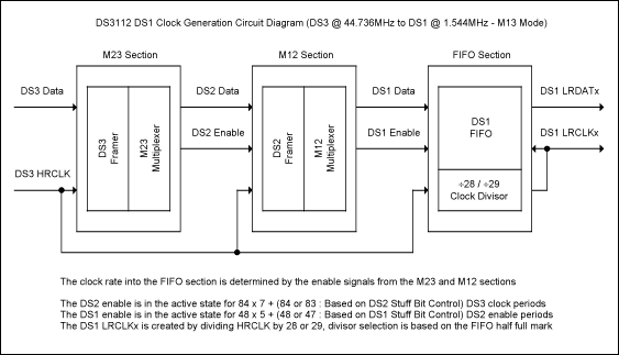
DS1 Clock Recovery for M13 and C-Bit Parity ModesThe recovery of the 28 individual DS1 clocks from the DS3 signal is a complex three-stage process.
The first stage, the M23 stage, demultiplexes the DS3 signal into seven individual DS2 signals. Instead of recovering the individual DS2 clocks, DS2 enables are created. Each of the seven DS2 enables is in the active state for 84 x 7 + (84 or 83) DS3 clock periods per DS3 frame. The decision to recover the final 84 or 83 DS3 clock periods is based on the DS2 Stuff Bit control.
The second stage is the M12 stage which demultiplexes each of the seven DS2 signals into four DS1 signals for a total of 28 DS1 signals. As in the M23 stage, the M12 stage does not recover the individual DS1 clocks, but instead creates DS1 enables. Each of the four DS1 enables is in the active state for 48 x 5 + (48 or 47) DS2 enable periods. The decision to recover the final 48 or 47 DS2 enable periods is based on the DS1 Stuff Bit control.
The third, and final, stage is the FIFO stage which actually recreates the individual DS1 clocks. Each of the DS1 clocks is created by dividing the DS3 clock (HRCLK) by either 28 or 29. The selection of the divisor is based on the amount of data currently stored in the FIFO. The FIFO uses the DS1 enable to write data into the FIFO and the DS1 clock (LRCLKx) to read data from the FIFO. The correct DS1 clock rate is recovered by the FIFO attempting to keep the amount of data in the FIFO centered at the half-full mark. If the amount of data is over the half-full mark, 'divide by 28' is chosen. If the amount of data is under the half-full mark, 'divide by 29' is chosen. A complete diagram of the clock-recovery mechanism is shown in Figure 1.

Figure 1. M13 and C-Bit parity modes.
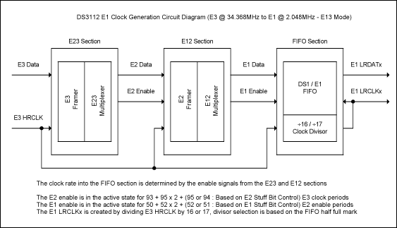
E1 Clock Recovery for E13 ModeThe recovery of the 16 individual E1 clocks from the E3 signal is also a complex three-stage process.
The first stage is the E23 stage which demultiplexes the E3 signal into four E2 signals. Instead of recovering the individual E2 clocks, E2 enables are created. Each of the four E2 enables is in the active state for 93 + 95 x 2 + (95 or 94) E3 clock periods per E3 frame. The decision to recover the final 95 or 94 E3 clock periods is based on the E2 Stuff Bit control.
The second stage is the E12 stage which demultiplexes each of the four E2 signals into four E1 signals for a total of 16 E1 signals. As in the E23 stage, the E12 stage does not recover the individual E1 clocks, but instead creates E1 enables. Each of the four E1 enables is in the active state for 50 + 52 x 2 + (52 or 51) E2 enable periods. The decision to recover the final 52 or 51 E2 enable periods is based on the E1 Stuff Bit control.
The third, and final stage, is the FIFO stage which actually recreates the individual E1 clocks. Each of the E1 clocks is created by dividing the E3 clock (HRCLK) by either 16 or 17. The selection of the divisor is based on the amount of data currently stored in the FIFO. The FIFO uses the E1 enable to write data into the FIFO and the E1 clock (LRCLKx) to read data from the FIFO. The correct E1 clock rate is recovered by the FIFO which attempts to keep the amount of data in the FIFO centered at the half-full mark. If the amount of data is over the half-full mark, 'divide by 16' is chosen. If the amount of data is under the half-full mark, 'divide by 17' is chosen. A complete diagram on the clock-recovery mechanism is shown in Figure 2.

Figure 2. E13 mode.
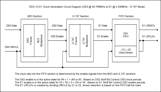
E1 Clock Recovery for G.747 ModeThe recovery of the 21 individual E1 clocks from the DS3 signal is also a complex three-stage process.
The first stage is the M23 stage which demultiplexes the DS3 signal into seven DS2 signals. Instead of recovering the individual DS2 clocks, DS2 enables are created. Each of the seven DS2 enables is in the active state for 84 x 7 + (84 or 83) DS3 clock periods per DS3 frame. The decision to recover the final 84 or 83 DS3 clock periods is based on the DS2 Stuff Bit control.
The second stage is the G.747 stage which demultiplexes each of the seven DS2 signals into three E1 signals for a total of 21 E1 signals. As in the M23 stage, the G.747 stage does not recover the individual E1 clocks but instead creates E1 enables. Each of the three E1 enables is in the active state for 53 + 55 x 3 + (55 or 54) DS2 enable periods. The decision to recover the final 55 or 54 DS2 enable periods is based on the E1 Stuff Bit control.
The third, and final, stage is the FIFO stage which actually recreates the individual E1 clocks. Each of the E1 clocks is created by dividing the DS3 clock (HRCLK) by either 21 or 22. The selection of the divisor is based on the amount of data currently stored in the FIFO. The FIFO uses the E1 enable to write data into the FIFO and the E1 clock (LRCLKx) to read data from the FIFO. The correct E1 clock rate is recovered by the FIFO which attempts to keep the amount of data in the FIFO centered at the half-full mark. If the amount of data is over the half-full mark, 'divide by 21' is chosen. If the amount of data is under the half-full mark, 'divide by 22' is chosen. A complete diagram on the clock-recovery mechanism is shown in Figure 3.

Figure 3. G.747 mode.
References
For further questions on the DS3112 low-speed clock recovery, please contact the Telecommunication Applications support team by email, telecom.support@dalsemi.com, or telephone at 01-972-371-6555.
For general information about the DS3112, please consult the data sheet.
欢迎分享,转载请注明来源:内存溢出

 微信扫一扫
微信扫一扫
 支付宝扫一扫
评论列表(0条)