IntroductionThis application note applies to the following products:
This application note will discuss the requirements for multiplexing four PCM streams into one 8MHz system backplane using Dallas Semiconductor SCTs and framers that do not contain interleave bus operation (IBO) functionality internally. > The DS2155, DS26528, DS26524, DS26522, DS26521, DS26519 and DS26518 all contain IBO functionality internally and do not need the extra logic shown below.
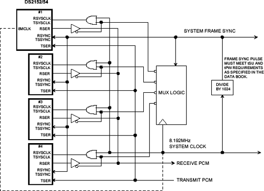
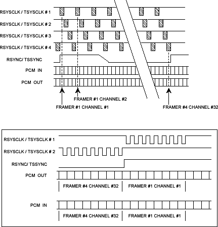
T1 or E1 PCM signals can interface to an 8MHz system backplane. Typically, this application is used to multiplex four PCM streams onto a single 8MHz PCM stream. To accomplish this, the elastic stores are enabled and placed in the 2.048MHz SYSCLK mode. Figure 1 illustrates a circuit in which a single SYNC signal is generated for all four framers. Each framer in turn is driven with an 8.192MHz clock burst of 8 cycles. Each clock burst causes the elastic store to output one DS0. This results in a byte-interleaved 8.192MHz PCM steam (see Figure 2).
Figures 1 and 2 apply to the DS2152 and DS2154. Figure 1 shows the 8.192MHz clock can optionally be derived from a master DS2152/54.

Figure 1.

Figure 2.
Master Clock SourceIn Figure 1, the 8.192MHz system clock may be derived from a T1/E1 line as indicated by the dotted line. This line becomes the timing master for the other three devices. In this example, device #1 is used as the master. The other three devices may experience frame slips since there is no guarantee that their inbound T1/E1 rates are synchronous to device #1's inbound rate. The elastic stores manage frame slip events in a logical manner by either repeating or deleting a full frame.
Master Clock FailureIn the event that the master line fails, the following events will occur. RCLK will be replaced by MCLK. If the jitter attenuator is enabled in the receive path, this transition will be very smooth. Consequently, the 8.192MHz clock output on the 8 MCLK pin will make a slight and smooth transition to be phase locked to the clock at MCLK. The 8.192MHz system timing will not experience any disturbance of the byte interleave structure. Device #1 will report a receive carrier loss (RCL) event via the status registers. When the host detects the failure of the master line, processor selection logic may be used to switch to another active line.
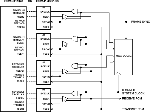
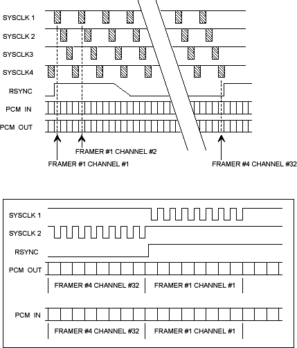
Figures 3 and 4 apply to the DS2141, DS21Q41, DS2143, DS21Q43, DS2151, and DS2153.

Figure 3.

Figure 4.
Backplane InformationIf you have further questions on backplane operation of our legacy T1/E1 products, please contact the Telecommunication Applications support team via email telecom.support@dalsemi.com or call 972-371-6555.
For more information about our legacy T1/E1 products, please consult the data sheets available on our website at www.maxim-ic.com/telecom.
欢迎分享,转载请注明来源:内存溢出

 微信扫一扫
微信扫一扫
 支付宝扫一扫
评论列表(0条)