OverviewThis applicaTIon note describes how to convert T1 to E1 or vice versa using Maxim Transceivers DS21X52 and DS21X54 single-chip transceivers (SCTs) with the DS216xx clock adapter (CLAD).
The Maxim DS21X52 SCT is used for T1 signals and the DS21354 is used for E1 signals. Any one of the three Maxim CLADs (DS21600, DS21602, or DS21610) can be used to convert the signal from T1 to E1 frequency or E1 to T1 frequency.
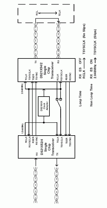
The diagram below illustrates how the connecTIons are made between the devices. RSYSCLK of DS21352 or DS21354 is connected with TCLK and RSYSCLK of DS21354 or DS21352. The signal from RCLK of DS21352 or DS21354 goes to CLKIN of the CLAD. The CLAD converts this signal and the output CLKOUT1 goes to TCLK and RSYSCLK of DS21354 or DS21352. For both transceivers, RSYNC is connected with the TSYNC of the other transceiver for synchronizaTIon.
The clock adapters that can be used for this application are as follows:
Table 1. Frequency Conversions (MHz)
0
1
2.048 2.048
1.544
0
1
2.048 2.048
1.544

Figure 1. Signal Conversion From T1 TO E1 Using DS216XX CLAD.
Elastic Store ModeWhen T1 signal (1.544MHz) from CLKOUT1 is connected to RSYSCLK pin, then every fourth channel of the received E1 data will be deleted and an F-bit position will be inserted. Hence, channels 1, 5, 9, 13, 17, 21, 25, and 29 (timeslots 0, 4, 8, 12, 16, 20, 24, and 28) will be deleted from the received E1 data stream. Also, in 1.544MHz applications, the RCHBLK output will not be active in channels 25 through 32 (or in other words, RCBR4 is not active). If the 512-bit elastic buffer either fills or empties, a controlled slip will occur. If the buffer empties, then a full frame of data (256 bits) will be repeated at RSER and the SR1.4 and RIR.3 bits will be set to a one. If the buffer fills, then a full frame of data will be deleted and the SR1.4 and RIR.4 bits will be set to a one.
If E1 signal (2.048MHz) CLKOUT1 is connected to the RSYSCLK pin, then the data output at RSER will be forced to all ones every fourth channel and the F—bit will be passed into the MSB of TS0. Hence, channels 1(bits 1-7), 5, 9, 13, 17, 21, 25, and 29 (timeslots 0, 4, 8, 12, 16, 20, 24, and 28) will be forced to a one. Also, in 2.048 MHz applications, the RCHBLK output will be forced high during the same channels as the RSER pin. If the 386-bit elastic buffer either fills or empties, a controlled slip will occur. If the buffer empties, then a full frame of data (193 bits) will be repeated at RSER and the SR1.4 and RIR1.3 bits will be set to a one. If the buffer fills, then a full frame of data will be deleted and the SR1.4 and RIR1.4 bits will be set to a one.
欢迎分享,转载请注明来源:内存溢出

 微信扫一扫
微信扫一扫
 支付宝扫一扫
评论列表(0条)